3D Integration and Wafer-Level Packaging
Heterogeneous 3D integration of semiconductor components is a main driver within the microelectronics industry towards higher integration complexity, enhanced system performance and economies of scale. Our technology offering of 3D integration and wafer-level packaging methods enables solutions for system integration of analog/mixed-signal integrated circuits , sensors and MEMS. These components are essential for the next-generation microelectronics products of our customers in the key markets automotive, industrial, medical and mobile communication.
Micro-Transfer-Printing technology enables 3D heterogeneous integration through vertical stacking of chips in a wafer-level process. These stacked components might originate from different source materials and manufacturing technologies, such as integrated circuits from different CMOS nodes, compound semiconductors, etc. As such, Micro-Transfer-Printing is a disruptive technology from which many novel applications will benefit.
Through-silicon vias are electrical interconnects between the front and back sides of a wafer. Our unique technology provides a TSV solution that is fully
integrated with our CMOS technologies and thereby enables innovative and cost-effective assembly concepts for analog/mixed-signal integrated circuits and sensors. Avoiding electrical connections on the top surface increases the effective chip area for sensor applications and enables a physical separation of electrical signals from the front side, for example in microfluidic devices.
CMOS–MEMS integration: Each sensor or actuator requires an integrated circuit for the processing of electrical input or output signals. For selected types of MEMS sensors and actuators, we offer solutions that are monolithically integrated with appropriate analog/mixed-signal CMOS nodes. We leverage the fact that X-FAB is at home in both worlds – CMOS and MEMS.
Our long-time experience with different wafer-level bonding techniques has enabled us to produce many types of sensors. In addition, we use wafer bonding for packaging chips, which generally reduces packaging costs, but can also add functionality, for example for capping microfluidic channels.
Our engineers love to develop challenging technologies together with our customers to come up with new integrated semiconductor solutions. Wafer-level packaging and 3D integration are among the specialties X-FAB focuses on.
Dr. Steffen Leopold, Technical Director BU MEMS
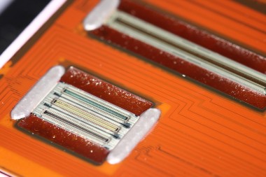
Micro-Transfer-Printing - Heterogeneous integration
Micro-Transfer-Printing (µTP) is an approach for the heterogeneous integration of microscale electronic devices on non-native substrates by means of stamp pick-up and printing procedures.
Advantages / Features:
- Parallel IC integration: highly efficient process
- Superior alignment accuracy
- Solutions for System-in-Package integration of CMOS, MEMS, wide-bandgap and photonic devices
Benefits:
- Heterogeneous integration – effective combination of different semiconductor materials
- Simultaneous “pick and place” of large amounts of chiplets
- Optimal use of expensive wafer materials
Our offering:
- Industry-first pilot line for the integration of smart systems by µTP
- Technology development and manufacturing solutions for heterogeneous system integration of CMOS, MEMS, wide-bandgap and photonic devices
- Dedicated process solutions to enable transfer printing of ASICs manufactured in our 180 nm CMOS node

Micro-Transfer-Printing – Application examples
ASIC integration enabling System-in-Package solutions
We offer a dedicated process solution for the heterogeneous integration of ASICs, using our XT018 SOI technology. Such printable SOI ASICs exhibit uniquely small feature sizes in both their lateral dimensions and their height. Along with the superior alignment accuracy and the scalability of a wafer-scale process, this technology unlocks a great potential for System-in-Package (SiP) solutions for many applications, including power management devices, radio frequency (RF) amplifiers, micro LED drivers and medical sensors. A special feature of transfer printing is the possibility to integrate chip arrays in a straightforward way.

Heterogeneous integration of GaAs Hall plates for magnetic sensors
For the heterogeneous combination of highly sensitive GaAs Hall plates with robust and reliable CMOS sensor ASICs and logics, a valuable process integration can be achieved by µTP. Print-ready GaAs Hall plates can thus be integrated directly on CMOS ASICs, allowing minimal package sizes and sensitivities up to five times higher than for state-of-the-art Si-based sensors.

Optical filters for photosensitive sensors
The integration of optical filters by µTP allows a more efficient use of expensive filter materials, as filter chiplets from one donor wafer can be used to populate multiple sensor wafers. It is also possible to integrate several different bandpass filters on one particular sensor ASIC.

µLED integration for ambient car lighting
As with the integration of Hall plates, µTP offers the possibility to integrate µLEDs directly on the LED driver ICs. This allows minimal package sizes to be achieved, reducing costs for our customers.

Printed Si photonics for life science and data center applications
For the integration of active photonic devices like µLEDs, lasers, photodiodes and modulators in passive waveguide circuits, µTP constitutes a very effective and highly precise integration technology. Thanks to the dense fabrication on four- and six-inch InP and GaAs donor wafers, the valuable active devices can be distributed over multiple target wafers with minimal displacements. This process integration will particularly benefit life science and data center applications.

Integrated compound semiconductor devices for power and RF applications
High-power, high-voltage and RF applications in particular will benefit from the integration of GaN high electron mobility transistors (HEMTs) and RF switches on reliable CMOS ASICs. As a wide-bandgap material, GaN offers superior performance to Si or SiC alternatives and can be used and integrated very effectively by µTP. Moreover, the removal of residual handle wafer material as well as very short metallization tracks improve the overall device performance.
3D interconnects – Through-silicon via
Through-silicon via (TSV) technology provides an innovative and efficient way to exploit the third dimension in wafer- and die-level 3D integration.
Advantages / Features:
- Vertical electrical connection (via) that passes completely through a silicon wafer or die
- High-performance interconnect techniques used as an alternative to wire bonding and flip chip to create 3D packages and 3D integrated circuit
- Substantially higher interconnect and device density and shorter length of connections compared to alternatives such as package-on-package
Benefits:
- Enables various packaging and form factor solutions
- Optimizes package form factor by avoiding wire bonds
- Improves front-side sensor access for light, gas, sound and liquid
- Enables stacking of chips for System-in-Package
- Allows tiling of image sensor chips
- Enables wafer-level chip-scale packaging (WLCSP)
Our offering:
- “TSVlast” process option for use in conjunction with our CMOS, CMOS sensors and MEMS technologies on 200 mm wafers
- "Low-density” TSV process to replace or augment top-side pads and wire bonding by bottom-side pads and a metal redistribution layer (RDL)
- Our TSV technology may be complemented by industry standard wafer- or die-level assembly methods like under-bump metallization (UBM) and solder ball placement.


3D packaging – Wafer bonding
Wafer bonding and wafer-level packaging (WLP) refer to various techniques for bonding two or more wafers together.
Advantages / Features:
- Direct, anodic, eutectic, glass frit and adhesive polymer bonding
- Used to form buried cavities, glass pedestals, protective covers and optical windows
- Silicon or glass wafers
- Eight- or six-inch silicon and glass caps
- Single or top and bottom caps
- Stack height up to 6 mm
- Wafer-level chip-scale packaging (WLCSP) used instead of traditional assembly techniques
Benefits:
- Same size of packaged device as ASIC device
- Possibility to test, characterize and stress devices in final packaging at wafer level
- Reduction of cost of packaging per chip
- Possibility to have controlled atmosphere (gas and pressure) in packaged device
Our offering:
- Wide range of wafer bonding experience and capabilities on eight-inch and six-inch wafers
- Processes available for direct, anodic, eutectic, glass frit and adhesive polymer bonding
- Wafer capping, optical windows, cavity formation, WLCSP
- In-production, open-platform processes featuring direct, anodic and glass frit wafer bonding
- Numerous customer-specific process developments completed
- Compatibility with MEMS wafer processing
- Combination of different materials with additional functionality


Related Resources
Contact

Stefan Ernst
Technical Marketing Manager
WLP & 3D Integration
For more information, please contact us: