
Silicon PhotonicsCombining the best of silicon and advanced photonics materials
At X-FAB, we’re redefining what’s possible in high-speed, low-power silicon photonics. By combining the scalability of CMOS manufacturing with the performance of III-V semiconductor materials, we’re pushing data transmission to new levels. Our platform integrates silicon-on-insulator (SOI) technology, low-loss silicon (Si) and silicon nitride (SiN) waveguides, high-efficiency electro-optic modulators, and cutting-edge grating couplers. Through heterogeneous integration, we bring together indium phosphide (InP), gallium arsenide (GaAs), germanium (Ge), and lithium niobate chiplets – creating a seamless ecosystem for ultra-fast, energy-efficient optical communication.
From datacenters and telecom to LiDAR, AR/VR, quantum computing, and even biomedical applications, XPH90 is just the beginning. The future of silicon photonics is wide open, and at X-FAB, we’re building an entire product family to meet the growing demand for faster, smarter, and more integrated solutions. Whether it’s enabling multi-terabit data streams, next-gen AI computing, or optical sensors that push the boundaries of precision – our technology is built to shape what’s next.
Solutions
Scalable SOI Photonics Solutions for High-Performance Optical Integration
Key Features:
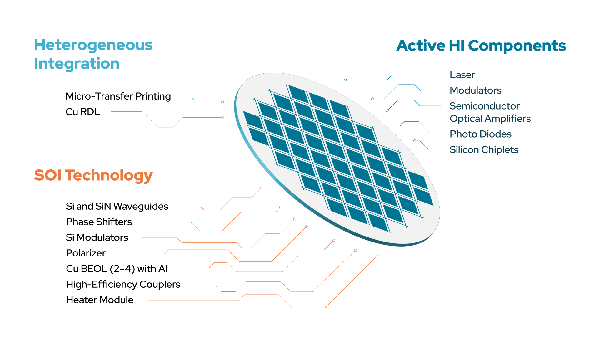
- Si and SiN Waveguides for low-loss, high-density optical routing
- Phase Shifters (thermal-optical, electro-optical) for precise signal control
- Si Modulators (MZI, ring) for high-speed optical data transmission
- Polarizer to enhance signal stability and minimize cross-talk
- Cu BEOL (2-4) with Al for high-speed RF interconnects and superior signal integrity
- High-Efficiency Couplers (grating, edge) for optimized light coupling
- Heater Module for fine-tuned wavelength stabilization and thermal tuning
User Benefits:
- Enables high-speed, energy-efficient optical communication
- Provides scalable, low-loss waveguides for photonic integrated circuits (PICs)
- Reduces power consumption through optimized thermal and electro-optic control
- Supports seamless integration with active photonic and RF components
- Ensures manufacturability and high-volume production readiness
Key Features:
- Micro-Transfer Printing for precise III-V material placement on SOI
- Cu RDL (Redistribution Layer) for high-density interconnects and packaging
User Benefits:
- Combines the advantages of III-V materials with SOI scalability
- Reduces power consumption while enhancing optical performance
- Enables compact, multi-functional photonic circuits with advanced packaging
- Supports cost-effective, high-yield wafer-level manufacturing
- Accelerates product development cycles with standardized integration flows
Key Features:
- Laser sources (InP, GaAs) for integrated on-chip light generation
- Modulators (electro-optic, thermal-optic) for high-speed optical data encoding
- Semiconductor Optical Amplifiers (SOAs) for signal boosting and low-noise transmission
- Photo Diodes (InP, SiGe) for high-sensitivity optical signal detection
User Benefits:
- Enables high-speed, low-latency optical communication for next-gen applications
- Reduces reliance on external optical sources, improving integration and scalability
- Optimized for telecom, datacom, LiDAR, and optical sensing applications
- Provides a compact, efficient, and high-performance solution for photonic systems
- Enhances signal integrity and system performance across a broad wavelength range
Download datasheet to learn more
Applications

Data Centers and Computing
Fast, efficient optical interconnects
High-speed Si and SiN waveguides enable low-loss signal transmission, while Si modulators and high-speed photodetectors optimize data processing. Heterogeneous integration of InP and GaAs chiplets ensures compact, energy-efficient optical interconnects, supporting AI, cloud computing, and multi-terabit data transmission.

Telecom
High-speed, low-power optical networks
Next-generation optical networks benefit from Si modulators (MZI, ring), high-speed photodetectors, and low-loss waveguides. Micro-transfer printing of III-V materials boosts data rates while reducing power consumption. Pluggable module solutions provide scalability for fiber networks, and 5G infrastructure.

Photonics LiDAR
Precision sensing for next-gen LiDAR
Advanced Si and SiN waveguides, high-speed modulators, and InP-based photodetectors enable precise signal control. Phase shifters and polarizers enhance accuracy, while heterogeneous integration improves resolution and range. Scalable manufacturing supports automotive, industrial automation, and AR/VR applications.



Related Resources
Contact
For more information, please contact us: