
Manufacturing Solutions
X-FAB has an established track record of over 30 years of experience providing proprietary manufacturing processes and advanced design and engineering support offerings. Excellent service, reliability and first-class technical support – that’s what X-FAB stands for.
X-FAB group operates six wafer manufacturing sites in Germany, France, Malaysia, and the United States. With its expertise in analog/mixed-signal technologies, microsystems/MEMS and silicon carbide (SiC), X-FAB is the development and manufacturing partner for its customers, primarily serving the automotive, industrial and medical end markets.
We ensure a long-term supply of more than 15 years and dual sourcing for our 350 nm technologies to provide our customers with long-term reliability and stability.
Damien Macq, CEO, X-FAB Group
The foundry in the semiconductor value chain
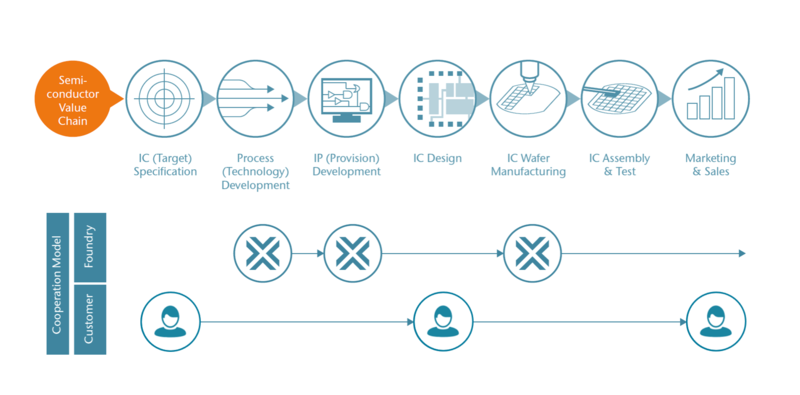
X-FAB manufactures analog/mixed-signal ICs utilizing proprietary process technologies. As a pure-play foundry X-FAB does not have its own IC products, but manufactures them based on designs created by its customers or third parties in cooperation and mostly based on X-FAB’s portfolio of modular, highly specialized proprietary process technologies and IP.
Sustainability
Sustainability embodies many different facets, from environmental care to health and safety, human rights, business ethics and social responsibility. Visit our sustainability webpage to find more information.
Manufacturing processes and capabilities
A modular approach allows customers to choose from a wide range of enhanced options across many semiconductor technologies, designs and processes including complementary metal-oxide semiconductor (CMOS), silicon on insulator (SOI), silicon carbide (SiC), gallium nitride (GaN) and micro-electro-mechanical systems (MEMS).
Customers can draw on a variety of features in order to develop ICs specifically tailored to their end-use requirements and to optimize product performance, product size, power consumption, and other parameters. Currently, we offer foundry process technologies with feature sizes of 1.0 μm and 0.8 μm on 150 mm wafers and 350 nm, 250 nm, 180 nm, 130 nm and 110 nm on 200 mm wafers.


Contact
For more information, please contact us: