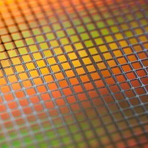
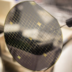
Our Technology Portfolio
As a pure-play foundry specialized in analog/mixed-signal applications, we offer a wide range of modular CMOS and SOI processes in geometries ranging from 1.0 µm to 130 nm as well as special MEMS and SiC process capabilities.
CMOS & SOI overview
Overview of X-FAB's CMOS and SOI process options ranging from 130 nm to 1.0 µm.
Digital | Analog Mixed Signal | High Voltage | NVM | RF | Opto | SOI | High Temp | |
|---|---|---|---|---|---|---|---|---|
1.0 µm |
|
|
|
|
|
|
| |
0.6 µm |
|
|
|
|
|
|
|
|
350 nm |
|
|
|
|
|
|
| |
180 nm |
|
|
|
|
|
|
|
|
130 nm |
|
|
|
|
| |||
110 nm |
|
|
|
|
|
|
X-FAB's CMOS process offering
Unlike most conventional semiconductor foundries, X-FAB does not simply stick to the ITRS Roadmap, trying to develop ever-smaller and faster CMOS process technologies.
The ITRS Roadmap is our guideline - our central aim, however, is to enhance and expand the CMOS technologies it recommends with additional, special analog functions and modular options.
X-FAB thus creates a broad range of new mixed-signal process families for applications in various areas, from the automotive and medical sector to industrial applications, communication products, or consumer electronics.
Our state-of-the-art CMOS and SOI platforms can be complemented with specialties ranging from analog/mixed-signal functions to high-voltage options, embedded non-volatile memories, optical, RF and bipolar elements, or the implementation of microelectromechanical sensor technologies.
180 nm CMOS process family
Automotive 180 nm sensor and high-voltage technology platform
XH018 is a powerful modular 180 nm sensor and high-voltage EPI technology. It combines the benefit of a 180 nm modular 1.8 V / 3.3 V ultra low noise process supporting an extended temperature range of -40 to 175°C with an extensive portfolio of high-voltage and analog devices as well as a range of automotive grade non-volatile memory options. In addition, multiple fully characterized photodiode and APD/SPAD options are available. The XH018 platform is designed for smart sensor, sensor interface and actuator applications.
Best-in-class PDK support for all major EDA vendors, extensive device characterization and modelling, comprehensive analog, digital, and memory IPs.Key features:
- Fully modular 180 nm EPI process based on 1.8 V / 3.3 V dual gate core module
- Up to six metal layers with different thick metal options
- Up to 175ºC operating temperature supporting AEC-Q100 grade 0
- Unique integration of digital, analog, HV and NVM in a single process
- High-reliability automotive NVM solutions including embedded Flash, NVRAM and OTP
- Optional ultra-low-noise 1.8 V and 3.3 V CMOS
- Fully characterized photodiodes and APD/SPAD
- 10 V to 45 V high-voltage CMOS transistors with 18 V gate oxide
- High gain BJTs
- HV Schottky diodes
- Standard and high capacitance single, double, triple MIM and metal fringe capacitors
- Multiple 1.8 V and 3.3 V libraries available to enable complex designs
- Comprehensive PDK support for Cadence, Siemens EDA, Synopsys and others
Automotive 180 nm high-voltage and analog/mixed-signal technology platform
XP018 is a modular 180 nm high-voltage EPI technology. It combines the benefit of a 180 nm 5 V based process supporting an extended temperature range of -40 to 175 °C with an extensive portfolio of high voltage and analog devices as well as a range of automotive grade non-volatile-Memory options. The XP018 platform is specifically designed for cost sensitive and robust automotive, industrial and medical applications.
Best-in-class PDK support for all major EDA vendors, extensive device characterization and modelling, comprehensive analog, digital, and memory IPs.Key features:
- Fully modular 180 nm EPI process based on low mask count 5 V single gate core module
- Up to six metal layers with different thick metal options
- Up to 175ºC operating temperature supporting AEC-Q100 grade 0
- Unique integration of digital, analog, HV and NVM in a single process
- High-reliability automotive NVM solutions including embedded Flash, EEPROM and OTP
- 12 V to 60 V high-voltage CMOS transistors
- High gain BJTs
- Schottky and Zener diodes
- Standard and high capacitance single, double, triple MIM and metal fringe capacitors
- Comprehensive PDK support for Cadence, Siemens EDA, Synopsys and others
180 nm image sensor technology platform
XS018 is X-FAB’s specialized process for fast image sensors and high-sensitive photodiodes. The optional available modules for 4 transistor cells, pinned photo diodes and the stitching capabilities make this technology ideal for large image sensor applications needing high frame rates as used for instance for medical and scientific X-ray cameras.
A photodiode-specific process-core module allows the realization of best-in-class UV-photodiodes as well as high-sensitive photodiode for ambient and near-infrared light. All major EDA vendors are supported. Extensive device characterization and modelling (also for photodiodes), comprehensive analog, digital, and memory IPs are available.
Key features:
- Fully modular 180nn EPI process based on low mask count 3.3V Single Gate core module
- 3.3V/1.8V core process options
- Up to six metal layers with different thick metal options
- Thin top metal option
- Pinned photodiode module with choice of 4 different pinning voltages
- Low threshold voltage NMOS with choice of 5 different threshold voltages
- Pixel reference designs from 3.6 to 200µm
- Six different photodiodes supporting UV, ambient and NIR light
- High value poly resistors
- Standard and High capacitance single, double, triple MIM and Metal Fringe capacitors
- Low noise depletion and buried channel transistors
- Support of 1D and 2D stitching
- Comprehensive PDK support for Cadence, Siemens EDA, Synopsys and others
Automotive 180 nm BCD-on-SOI technology platform
XT018 is X-FAB’s premier 180 nm modular high-voltage BCD-on-SOI technology. It combines the benefit of SOI wafers with Deep Trench Isolation (DTI) and those of a state-of-the-art six metal layers 180 nm process. XT018 features a complete portfolio of voltage options from 10 V to 200 V as well as a full range of automotive Grade-0 qualified Non-Volatile-Memory options.
The XT018 platform is specifically designed for a next generation automotive, industrial and medical applications operating in the temperature range of -40 to 175 °C.
Best-in-class PDK support for all major EDA vendors, extensive device characterization and modeling, comprehensive set of analog, digital, and memory IPs.Key features:
- Fully modular 180 nm SOI process based on low mask count 5 V Single Gate core module
- Up to six metal layers with different thick metal options
- Deep Trench Isolation and handle wafer contact
- Up to 175 ºC operating temperature supporting AEC-Q100 Grade 0
- Unique integration of digital, analog, HV, NVM and SOI in a single process
- High-reliability automotive NVM solutions including embedded Flash, EEPROM and OTP
- 10 V to 200 V high-voltage CMOS transistors
- Excellent specific Ron HV N-channel device performance
- High gain BJTs
- Very fast forward HV, Schottky and Zener diodes
- Standard and high capacitance single, double, triple MIM and metal fringe capacitors
- Comprehensive PDK support for Cadence, Siemens EDA, Synopsys and others
- Silicon Frontline R3D support for metal optimization
350 nm CMOS process family
With our 350 nm process family you can design chips for a wide range of applications. All four processes come with best-in-class PDK support for all major EDA vendors, extensive device characterization and modelling as well as comprehensive analog, digital, and memory IPs.
Comprehensive 350 nm sensor and high-voltage technology platform
XH035 is a comprehensive modular 350 nm sensor and high-voltage EPI technology. It combines the benefit of a 350 nm modular 3.3 V ultra low noise process with an extensive portfolio of high voltage and analog devices. The XH035 platform is designed for robust sensor and sensor interface applications.
Best-in-class PDK support for all major EDA vendors, extensive device characterization and modelling, comprehensive analog, digital, and memory IPs.Key features:
- Fully modular 350 nm EPI process based on 3.3 V ultra low noise core module
- Alternative 5 V core module or 3.3 V / 5 V dual gate
- Best-in-class ultra low noise 3.3 V PMOS
- Up to four metal layers with thick metal options
- Up to 125 ºC operating temperature supporting AEC-Q100 grade 1
- Unique integration of digital, analog, HV and NVM in a single process
- High-reliability automotive NVM solutions including EEPROM
- Optical window etching and Anti Reflecting Coating for high sensitive photodiodes
- 10 V – 100 V HV CMOS transistors with 3.3 V, 5 V or 18 V Gate Oxide
- High gain BJTs
- HV Schottky diodes
- Standard single, double MIM, Poly and metal fringe capacitors
- Comprehensive PDK support for Cadence, Siemens EDA, Synopsys and others
Comprehensive 350 nm automotive sensor and high-voltage technology platform
XA035 is a comprehensive modular 350 nm sensor and high-voltage EPI technology. It combines the benefit of a 350 nm modular 3.3 V ultra low noise process supporting an extended temperature range of -40 to 175 °C with an extensive portfolio of high voltage and analog devices. The XA035 platform is designed for robust automotive sensor, sensor interface and actuator applications.
Best-in-class PDK support for all major EDA vendors, extensive device characterization and modelling, comprehensive analog, digital, and memory IPs.Key features:
- Fully modular 350 nm EPI process based on 3.3 V ultra low noise core module
- Optional 3.3 V / 5 V dual gate
- Best-in-class ultra low noise 3.3 V PMOS
- Up to four metal layers with thick metal options
- Up to 175 ºC operating temperature supporting AEC-Q100 grade 0
- Unique integration of digital, analog, HV and NVM in a single process
- High-reliability automotive NVM solutions including EEPROM
- Optical window etching and Anti Reflecting Coating for high sensitive photodiodes
- 10 V – 100 V HV CMOS transistors with 3.3 V, 5 V or 18 V Gate Oxide
- High gain BJTs
- HV Schottky diodes
- Standard single, double MIM, Poly and Metal Fringe capacitors
- Comprehensive PDK support for Cadence, Siemens EDA, Synopsys and others
350 nm modular sensor technology platform
XO035 is X-FAB’s specialized process for high-speed optoelectronics. It is especially suited for applications needing high-sensitive high- bandwidth photo diodes arrays for such as optical data storage, optical data communication or high dynamic range sensors. Special opto-process modules allow an optimised PIN cathode implantation, optical window etching and dedicated ARC layer deposition.
Best-in-class PDK support for all major EDA vendors, extensive device characterization and modelling, comprehensive analog, digital, and memory IPs.Key features:
- Fully modular 350 nm EPI process based on 3.3V core module
- Alternative 5 V module
- Up to four metal layers with different thick metal options
- High-sensitive PIN photodiodes
- Optical window etching and Anti Reflecting Coating optimized for different wavelengths
- High gain BJTs
- Standard single, double MIM, Poly and metal fringe capacitors
- Comprehensive PDK support for Cadence, Siemens EDA, Synopsys and others
0.6 µm to 1 µm CMOS process families
X-FAB offers a range of mature CMOS process in the 0.6 µm to 1 µm process nodes that come with specialties like high-temperature capability, enhanced voltage range and many modular process options to fit your device needs. All of these processes come with best-in-class PDK support for all major EDA vendors, extensive device characterization and modelling as well as comprehensive analog, digital, and memory IPs.
0.6 µm automotive sensor and high-voltage technology platform
XC06 is a comprehensive modular 0.6 µm sensor and high-voltage EPI technology. It combines the benefit of a 0.6 µm modular 5 V process with an extensive portfolio of high voltage, analog devices and non-volatile memory options. The XC06 platform features fast PIN diode and is well suited for automotive, industrial and medical applications. Best-in-class PDK support for all major EDA vendors and a complete set of analog, digital, and memory IPs.
Key features:- Modular 0.6 µm 5 V single poly, double metal core process
- Up to 3 metal layers with thick power metal option
- Up to 2 poly layers with CAPRES option
- Up to 125 ˚C operating temperature supporting AEC-Q100 Grade 1
- Unique integration of digital, analog, HV and NVM in a single process
- 8 V – 60 V HV CMOS transistors with 18 V Gate Oxide
- HV JFET
- High-reliability automotive NVM solutions including EEPROM and Flash
- High Gain Vertical PNP and NPN BJTs
- HV BJTs
- Schottky diode
- Integrated fast PIN photodiodes
- Comprehensive PDK support for Cadence, Siemens EDA, Synopsys and others
0.6 µm modular BCD-on-SOI technology platform
XT06 is X-FAB’s mature 0.6 µm modular high-voltage BCD-on-SOI technology. It combines the benefit of SOI wafers with Deep Trench Isolation (DTI) and an cost effective 0.6 µm 3 metal layers process. XT06 features high-voltage primitive devices from 8 V to 60 V as well as a range of non-volatile memory options with operating temperature range of -40 to 125 °C.
Best-in-class PDK support for all major EDA vendors, extensive device characterization and modelling, comprehensive analog, digital, and memory IPs.Key features:
- Modular 0.6 µm 5 V single poly core process
- Up to 3 metal layers with thick power metal option
- 8 V, 12 V, 30 V and 60 V HV transistors with 18 V gate oxide
- 8 V and 30 V depletion devices
- Vertical PNP and NPN BJTs
- Protection, rectifier and schottky diodes
- 60 V resistors and capacitors
- EasyFuse and EEPROM NVM IP options
- Comprehensive PDK support for Cadence, Siemens EDA, Synopsys and others
0.6 µm modular CMOS technology
XB06 is X-FAB’s mature 0.60 µm modular BiCMOS technology. It is a cost effective 0.60 µm 3 metal layers process with excellent analogue performance and accurate device matching. XB06 features a large number of bipolar primitive devices, high voltage primitive devices up to 30 V as well as a range of non-volatile memory options with operating temperature range of -40 to 125 °C. XB06 supports high speed optical sensors with PIN photodiodes.
Best-in-class PDK support for all major EDA vendors and a complete set of analog, digital, and memory IPs.Key features:
- Modular 0.60 µm 5 V double poly core process
- Up to 3 metal layers with thick power metal option
- 12 V and 30 V HV transistors with 15 V gate oxide
- 5 V and 30 V depletion devices
- High performance vertical and lateral PNP & NPN BJTs
- MIM and PIP capacitors
- Schottky diodes
- N-channel JFET
- EPROM and fuse NVM IP options
- Integrated fast PIN photodiodes
- Comprehensive PDK support for Cadence, Siemens EDA, Synopsys and others
SOI processes
130 nm RF SOI platform
The XR013 is X-FAB’s 130nm modular and feature-rich RF-SOI technology solution suitable for multiple air-interface standards and both fixed and mobile applications operating in the temperature range of -40 to 125°C. Standard features include a twin-well 2.5 V CMOS technology on a linear, high-impedance SOI substrate with 4 levels of metal in a hybrid copper and aluminum metallization that supports wire-bond, bump, or Cu-pillar chip-package interfaces and a large array of passive analog RF devices. Additional optional features include a range of FET devices including multiple Vt options, up to 2 additional routing, and up to 2 additional thick Cu metal levels.
Globally, the platform offers flexibility to customize and create cost-effective configurations with few mutually exclusive features. XR013 offers a full PDK support for major EDA vendors, comprehensive set of components supported by Si-proven, advanced RF models as well as a wide range of IP as design enablers.Key features:
- Low Ron * Coff figure of merit RF switches with PSP based compact models including advanced modelization of a high impedance SOI substrate
- Low-noise, high gain, high linearity NFET options for RF switch and LNA integration
- 2.5 V CMOS platform with hybrid Cu/Al metallization. Thick terminal metal is standard
- Both low and high value diffusion and poly resistors including a 3 kW/sq p-poly resistor
- 2.1 fF/µm² vertical RF Metal-Insulator-Metal capacitor and up to 1.32 fF/µm² Vertical parallel plate capacitors
- 1.2 V and 2.5 V based RF varactors
- Optional thick Cu levels provide a high-performance pathway to minimize system losses
- Large catalog of high-Q, symmetric, octagonal inductors for multiple metallization configurations
- Optional low-leakage 1.2 V CMOS feature is exploited to deliver best in class density digital integration
- Si proven RF reference kits
- Si proven analog & digital IP, Efuse and supporting IP
- Si proven GPIO libraries including ESD solutions
Automotive 180 nm BCD-on-SOI technology platform
XT018 is X-FAB’s premier 180 nm modular high-voltage BCD-on-SOI technology. It combines the benefit of SOI wafers with Deep Trench Isolation (DTI) and those of a state-of-the-art six metal layers 180 nm process. XT018 features a complete portfolio of voltage options from 10 V to 375 V as well as a full range of automotive grade-0 qualified non-volatile memory options.
The XT018 platform is specifically designed for a next generation automotive, industrial and medical applications operating in the temperature range of -40 to 175 °C.
Best-in-class PDK support for all major EDA vendors, extensive device characterization and modeling, comprehensive set of analog, digital, and memory IPs.Key features:
- Fully modular 180 nm SOI process based on low mask count 5 V Single Gate core module
- Up to six metal layers with different thick metal and CuRDL options
- Deep Trench Isolation and Handle Wafer Contact
- Up to 175 ºC operating temperature supporting AEC-Q100 Grade 0
- Unique integration of digital, analog, HV, NVM and SOI in a single process
- High-reliability automotive NVM solutions including Flash
- 10 V - 375 V HV CMOS transistors
- Excellent specific Ron HV N-channel device performance
- High gain BJTs
- Very fast forward HV, Schottky and Zener diodes
- Standard and High capacitance single, double, triple MIM and Metal Fringe capacitors
- Comprehensive PDK support for Cadence, Siemens EDA, Synopsys and others
- Silicon Frontline R3D support for metal optimization
0.6 µm modular BCD-on-SOI technology platform
XT06 is X-FAB’s mature 0.6 µm modular high-voltage BCD-on-SOI technology. It combines the benefit of SOI wafers with Deep Trench Isolation (DTI) and an cost effective 0.6 µm process. XT06 features high-voltage primitive devices from 8 V to 60 V as well as a range of non-volatile memory options with operating temperature range of -40 to 125 °C.
Best-in-class PDK support for all major EDA vendors, extensive device characterization and modelling, comprehensive analog, digital, and memory IPs.Key features:
- Modular 0.6 µm 5 V single poly core process
- Up to 3 metal layers with thick power metal option
- 8 V, 12 V, 30 V and 60 V HV transistors with 18 V gate oxide
- 8 V and 30 V depletion devices
- Vertical PNP and NPN BJTs
- Protection, rectifier and Schottky diodes
- 60 V resistors and capacitors
- EasyFuse and EEPROM NVM IP options
- Comprehensive PDK support for Cadence, Siemens EDA, Synopsys and others
1 µm 90 V 225 ˚C SOI technology platform
XI10 is a robust dielectric trench insulated 90 V technology solution supporting up to 225 ˚C junction temperature. The 13 layers 90 V core process module provides trench insulation, single level poly and 3 level of metal.
Best-in-class PDK support for all major EDA vendors, extensive device characterization and modelling, digital and memory IPs.Key features:
- 1 µm single poly 3 metal core process
- 5 V CMOS transistors
- 40 V, 60 V and 90 V NMOS and 30 V and 40 V PMOS transistors
- High temperature Tungsten metalization option
- Comprehensive PDK support for Cadence, Siemens EDA, Synopsys and others
1 µm modular 625V BCD-on-SOI technology platform
XDH10 is a robust dielectric trench insulated Ultra High Voltage (UHV) technology solution. The modular process provides a wide variety of passive, MOS and bipolar devices with dielectric bi-directional high voltage trench insulation. The 14 layers 625 VOP core process module provides trench insulation, single level poly with thick gate oxide and a third level metal with power metal.
Best-in-class PDK support for all major EDA vendors, extensive device characterization and modelling, comprehensive analog, digital, and memory IPs.Key features:
- Modular 1 µm single poly 3 metal core process
- 5 V and 7 V CMOS transistors
- 15 V , 20 V and 32 V NMOS and 20 V PMOS transistors
- Scalable UHV NDMOS & PMOS transistors
- 600 V IGBT
- High performance NPN and PNP transistors with up to 600 VCE
- 7 V and UHV depletion transistors
- Schottky and Zener diodes
- 650 V capacitor and resistor
- Comprehensive PDK support for Cadence, Siemens EDA, Synopsys and others
1 µm modular 340 V BCD-on-SOI technology platform
XDM10 is a robust dielectric trench insulated Ultra High Voltage (UHV) technology solution. The modular process provides a wide variety of passive, MOS and bipolar devices with dielectric bi-directional high voltage trench insulation. The 14 layers 340 VOP core process module provides trench insulation, single level poly with thick gate oxide and a third level metal with power metal.
Best-in-class PDK support for all major EDA vendors, extensive device characterization and modelling, comprehensive analog, digital, and memory IPs.Key features:
- Modular 1 µm single poly 3 metal core process
- 5 V and 7 V CMOS transistors
- 15 V , 20 V and 32 V NMOS and 20 V PMOS transistors
- Scalable UHV NDMOS & PMOS transistors
- 340 V IGBT
- High performance NPN and PNP transistors with up to 330 VCE
- 7 V and UHV depletion transistors
- Schottky and Zener diodes
- 350 V capacitor and resistor
- Comprehensive PDK support for Cadence, Siemens EDA, Synopsys and others
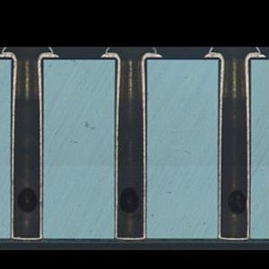
MEMS
X-FAB MEMS Foundry offers unsurpassed experience, expertise and execution with its high-volume MEMS manufacturing service. As the first ever pure-play MEMS foundry, X-FAB draws on more than 20 years MEMS manufacturing experience and continues to meet the new demands for this rapidly expanding and exciting group of technologies in terms of time to market, quality assurance, high yield and supply-chain management tools.
Operating from six fabs for MEMS and CMOS processes and an ecosystem of manufacturing and design partners, X-FAB is the proven choice for process development and installation, process capability, design support and long-term manufacturing stability.
As well as customer specific process installation, X-FAB offers a range of in-production standard process blocks, open-platform processes and IP blocks for key MEMS applications that enable fast time to market.
X-FAB MEMS Foundry offers an established, fast and professional service for contract manufacturing of MEMS and micro-machined structures that can grow with your high-volume business. Specific solutions are available for:
X-FAB's MEMS manufacturing is now focused on two locations, Erfurt and Itzehoe, both in Germany. However, X-FAB leverages the operations of all six of its manufacturing sites for the manufacturing of MEMS, which complements X-FAB’s other foundry solutions addressing optical, CMOS analog/mixed-signal and high voltage applications. A core competency of X-FAB is the monolithic integration of MEMS devices with CMOS technology to meet size and performance requirements. X-FAB also offers access to one of the broadest range of manufacturing materials in the semiconductor industry.
SiC & GaN
X-FAB is the first pure-play foundry to provide comprehensive processing technologies for wide bandgap (WBG) materials Silicon Carbide (SiC) and Gallium Nitride (GaN). We are offering foundry services for those new materials on the scale of silicon, using the existing silicon manufacturing lines. We are processing GaN-on-Si wafers in our modern 8” fab in Dresden, Germany and SiC wafers in our 6” fab in Lubbock, Texas, USA. By running the non-silicon wafers on the same lines as Si-wafers, our customers have access to high-quality and cost-effective foundry solutions. It allows customers to import their projects into a stable and trusted, fully automotive-qualified fab environment which supports output levels that are comparable with silicon yields.
X-FAB has a long history in processing SiC and GaN, ranging back to early 2013, with just a few customers starting to engage with those “exotic” materials. In this time, we gained significant knowledge and expertise and developed a business model that allows even less experienced customers to create their own SiC power devices or GaN HEMT devices.
With our sites in Dresden and Lubbock focused on serving the growing markets, the company is fully prepared for the expected acceleration of SiC and GaN device shipments – enabling key applications, such as charging applications, electric vehicles and advanced power management systems.
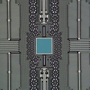
Heterogeneous Integration
Heterogeneous 3D integration of semiconductor components is a main driver within the microelectronics industry towards higher integration complexity, enhanced system performance and economies of scale. Our technology offering of 3D integration and wafer-level packaging methods enables solutions for system integration of analog/mixed-signal integrated circuits, sensors and MEMS. These components are essential for the next-generation microelectronics products of our customers in the key markets automotive, industrial, medical and mobile communication.
Contact
For more information, please contact us: