XT018 - The leading 180 nm BCD-on-SOI technology for your application needs
XT018 is our leading 180 nm BCD-on-SOI technology solution supporting automotive AEC-Q100 Grade 0 designs. It is a comprehensive modular platform with a complete portfolio of different voltage options – covering a 10 V to 375 V operating voltage range, depletion transistors, complementary high-performance and high-voltage bipolar transistors, Schottky diodes, Zener diodes
and a breadth of additional analog devices. 1.8 V multi-Vt options enable optimized designs in terms of power, performance and area. Numerous automotive-qualified memory options are also available, including SONOS-based Flash and embedded EEPROM.
Applications
- Automotive Battery Management ICs

Your best choice for Automotive Battery Management ICsKey challenges for automotive battery management IC designers are isolating precision analog circuits from other noisier parts of the IC and the handling of stringent automotive latch-up requirements while pushing the layout to a compact size.
One of the most important functional blocks of battery management ICs is the ADC. Its effective performance over the entire operating range is paramount to reliably measuring the voltages of battery cells. Noise from other functional blocks can compromise ADC performance. Thanks to its SOI/DTI isolation, XT018 greatly enhances the noise immunity of circuits that reside in their “own separate substrate”. Another aspect of the BCD-on-SOI process architecture is that it reduces junction leakage at elevated temperatures, which in turn improves ADC accuracy.
AEC-Q100 stipulates very stringent IC latch-up test specifications. Fulfilling these with bulk processes is a challenging design task. This is further aggravated as high-voltage parasitic devices are often not sufficiently modeled. With its SOI/DTI isolation, XT018 can completely eliminate latch-up, as there are no parasitic junctions between N-type and P-type devices that are placed in separate tubs.
Thanks to its SOI/DTI isolation, XT018 allows for a more compact layout compared to bulk processes. The tight DTI spacing enables significant area savings. No complicated biased single or double HV guard rings are required. Simplified circuit layout is often possible by taking full advantage of the BCD-on-SOI benefits. An example is the use of forward-biased diodes.
XT018 provides full PDK support for all major EDA vendors, extensive device characterization and modeling as well as a comprehensive range of analog, digital and memory IPs. Offered ESD cell libraries include low-voltage and high-voltage HBM ESD protection cells with high ESD robustness. Other powerful X-FAB design tools are the X-FAB ESD Design Checker (XESDC) and RelXplorer.
XESDC finds a set of possible ESD discharge current paths between the given chip pins of the design based on the official HBM standard. The RelXplorer is an interactive application that provides information about device and layer reliability according to application-specific mission profiles. It addresses all aspects of lifetime parameters and lifetime plots for MOS transistors, capacitors, dielectrics and interconnects.
- Industrial Interface ICs

Your best choice for Industrial Interface ICsKey challenges for industrial interface IC designers include handling reverse polarity conditions and shielding sensitive analog and digital blocks from other “noisy” functional blocks. A reduced die size without compromising product features or performance opens up the option to select smaller and cheaper packages.
Industrial I/O buses have to function reliably in very harsh factory environments. This also means that industrial interface ICs need to incorporate effective protection against over-voltages and reverse polarity events. Thanks to its SOI/DTI architecture, XT018 greatly simplifies the implementation of such protection. In addition, X-FAB provides an extensive ESD cell library, which includes special latch-up-robust ESD clamps suitable for reverse voltages. With these benefits, XT018 effectively enables first-time-right designs.
Isolating sensitive analog and digital blocks from other functional blocks is often a challenge. With its SOI/DTI isolation, XT018 greatly enhances the noise immunity of circuits that reside in their “own separate substrate”. Multi-channel implementations also become much easier to realize with this feature, which effectively reduces cross-talk.
The SOI/DTI isolation of XT018 also allows for a more compact layout compared to bulk processes. The tight DTI spacing enables significant area savings. No complicated biased single or double HV guard rings are required. Simplified circuit layout is often possible by taking full advantage of the BCD-on-SOI benefits. An example is the use of forward-biased diodes.
XT018 provides full PDK support for all major EDA vendors, extensive device characterization and modeling as well as a comprehensive range of analog, digital and memory IPs. Offered ESD cell libraries include low-voltage and high-voltage ESD protection cells with high ESD robustness. Other powerful X-FAB design tools are the X-FAB ESD Design Checker (XESDC) and RelXplorer.
XESDC finds a set of possible ESD discharge current paths between the given chip pins of the design based on the official HBM standard. The RelXplorer is an interactive application that provides information about device and layer reliability according to application-specific mission profiles. It addresses all aspects of lifetime parameters and lifetime plots for MOS transistors, capacitors, dielectrics and interconnects.
- Medical Ultrasound Tx/Rx ICs

Your best choice for Medical Ultrasound Tx/Rx ICsKey challenges for designers of medical ultrasound Tx/Rx ICs include availability of complementary low-Rds(on) high-voltage devices and the protection of sensitive analog and digital blocks from other “noisy” functional blocks. In addition, below-ground supply voltages need to be managed.
State-of-the-art medical ultrasound Tx/Rx designs require a range of well-matched NMOS and PMOS high-voltage primitive devices up to an operating voltage of 200 V. XT018 offers such complementary high-voltage primitive devices, which have low-Rds(on) performance and are fully floatable.
Managing below-ground supply voltages is another challenge, as ultrasound transmitters need to drive the piezo actuators with positive and negative voltages. With its SOI/DTI architecture, XT018 considerably simplifies the implementation.
Medical ultrasound TX/Rx designs consist of high-voltage, high-density digital and analog blocks. Isolating the sensitive analog and digital blocks from other functional blocks is often a challenge. Thanks to its SOI/DTI isolation, XT018 greatly enhances the noise immunity of circuits that reside in their “own separate substrate”. This feature also significantly reduces cross-talk in multi-channel Tx/Rx implementations in a very area-efficient way.
XT018 provides full PDK support for all major EDA vendors, extensive device characterization and modeling as well as a comprehensive range of analog, digital and memory IPs. Offered ESD cell libraries include low-voltage and high-voltage HBM ESD protection cells with high ESD robustness. Other powerful X-FAB design tools for ultrasound TX/Rx designs are the PowerMetal pcell and a range of multi-Vt standard cell libraries.
Applications with higher operating currents are exposed to higher mechanical stress. The XT018 PowerMetal pcell supports the layout designer by reducing the effort required to draw the complex metal interconnections. The layout created by the PowerMetal pcell helps to minimize the effective mass flux in the metal interconnections. A higher stability will be reached by an ideal design.
Digital performance is mainly determined by the speed of the switching edges, which in turn depends on the threshold voltage. XT018 comes with a number of compatible multi-Vt standard cell libraries, which provide additional flexibility for designers to balance the power and speed of their digital blocks.
- CAN FD Transceivers

XT018 – Your best choice for CAN FD TransceiversKey challenges for designers of CAN FD transceivers include handling negative transients as well as shielding sensitive analog and digital blocks from other “noisy” functional blocks. Achieving the smallest die size without compromising product features or performance is another critical aspect.
CAN FD transceivers have to support high data rates up to 5 Mbit/s in harsh environments. Achieving a proper bus fault protection up to ±70 V as well as IEC compatibility is essential. With its SOI/DTI architecture, XT018 greatly simplifies the implementation of such protection. Negative voltages can be easily handled.
Isolating sensitive analog and digital blocks from other functional blocks is often a challenge in bulk/BCD technologies. Thanks to its SOI/DTI isolation, XT018 greatly enhances the noise immunity of circuits that reside in their “own separate substrate”. Any noise on the CANL, CANH and supply pins can be effectively contained.
With its SOI/DTI isolation, XT018 allows for a more compact layout compared to bulk processes. The tight DTI spacing enables significant area savings. No complicated biased single or double HV guard rings are required. Simplified circuit layout is often possible by taking full advantage of the BCD-on-SOI benefits. An example is the use of forward-biased diodes for the CAN output stage.XT018 provides full PDK support for all major EDA vendors, extensive device characterization and modeling as well as a comprehensive range of analog, digital and memory IPs. Offered ESD cell libraries include low-voltage and high-voltage HBM ESD protection cells with high ESD robustness. The feature-rich XT018 PDK enables electromigration and IR-drop analysis as well as voltage-dependent checks.
Electromigration can cause fatal long-term reliability failures. Hence, accurate, simulation-based electromigration and IR-drop analysis is advisable. X-FAB supports this through silicon-proven design reference kits.
Primitive devices operating at different voltage classes must be properly separated and protected. The XT018 PDK supports LVS checks for coincidence, and the DRC ensures correct spacing related to the voltage class. Dynamic Rule Distance (DRD) shows layout designers if there are any design rule issues. The provided Operating Condition Check (OCC) verifies whether all primitive devices are operating within the permitted ranges, in particular with regard to voltage limitations defined within the technology specifications. - µLED Driver ICs
XT018 – Your best choice for µLED Driver ICsKey challenges for designers of µLED driver ICs include the integration of high-voltage and low-voltage analog blocks in a very small layout footprint. Subsequent post-processing will see the ICs thinned down significantly to make their height similar to the surrounding µLEDs.
With its SOI/DTI isolation, XT018 allows for a more compact layout compared to bulk processes. The tight DTI spacing enables significant area savings. No complicated biased single or double HV guard rings are required. Simplified circuit layout is often possible by taking full advantage of the BCD-on-SOI benefits, which further helps to reduce the die size.
XT018 offers low-Rds(on) high-voltage primitive devices supporting small footprint of high-voltage driver circuits. A range of high-density capacitor options up to 6.6 fF/µm2 is also available.
The BOX layer of XT018 can be very beneficial for the required post-processing steps. It can function as a natural etch stop layer while also providing additional stability to the ultrathin dies. In addition, XT018 offers special flat planarization options for the chip passivation surface.
XT018 provides full PDK support for all major EDA vendors, extensive device characterization and modeling as well as a comprehensive range of analog, digital and memory IPs. Offered ESD cell libraries include low-voltage and high-voltage HBM ESD protection cells with high ESD robustness.
Primitive devices operating at different voltage classes must be properly separated and protected. The XT018 PDK supports LVS checks for coincidence, and the DRC ensures correct spacing related to the voltage class. Dynamic Rule Distance (DRD) shows layout designers if there are any design rule issues. The provided Operating Condition Check (OCC) verifies whether all primitive devices are operating within the permitted ranges, in particular with regard to voltage limitations defined within the technology specifications.
Applications with higher operating currents are exposed to higher mechanical stress. The XT018 PowerMetal pcell supports the layout designer by reducing the effort required to draw the complex metal interconnections. The layout created by the PowerMetal pcell helps to minimize the effective mass flux in the metal interconnections. A higher stability will be reached by an ideal design.
- High-Voltage Audio ASICs

XT018 – Your best choice for High-Voltage Audio ASICsKey challenges for designers of high-voltage (HV) audio ASICs include the protection of sensitive analog and digital blocks from other “noisy” functional blocks as well as the availability of low-R(ds)on high-voltage and high-qualify bipolar devices while pushing the layout to a compact size.
HV audio ASIC designs consist of high-voltage, high-density digital and analog blocks. Isolating the sensitive analog and digital blocks from other functional blocks is often a challenge. Thanks to its SOI/DTI isolation, XT018 greatly enhances the noise immunity of circuits that reside in their “own separate substrate”. This feature also significantly reduces cross-talk in multi-channel implementations.
Designing HV audio ASICs requires a range of well-matched NMOS and PMOS high-voltage primitive devices. XT018 offers such high-voltage primitive devices up to 200 V, which come with low R(ds)on performance and can be floated for high-side configurations. In additional, high-performance complementary low-voltage and high-voltage bipolar primitive devices are available.
With its SOI/DTI isolation, XT018 allows for a more compact layout compared to bulk processes. The tight DTI spacing enables significant area savings. No complicated biased single or double HV guard rings are required. Simplified circuit layout is often possible by taking full advantage of the BCD-on-SOI benefits.
XT018 provides full PDK support for all major EDA vendors, extensive device characterization and modeling as well as a comprehensive range of analog, digital and memory IPs. Offered ESD cell libraries include low-voltage and high-voltage HBM ESD protection cells with high ESD robustness.
Accurate SPICE models are an essential ingredient for good circuit designs, enabling designers to check the integrity of their designs and predict circuit behavior. X-FAB is proud to provide best-in-class models with focus on analog devices that come with superior model quality and matching models to enable first-time-right designs.
XT018 comes with different NVM IP solutions for analog trimming. These include EasyFuse, TrimOTP and CEEPROM, which offer densities from 2 bit to 16 kbit. All three options are very cost-effective and do not require any additional mask layers. - Piezoelectric Haptic Driver ICs

XT018 – Your best choice for Piezoelectric Haptic Driver ICsKey challenges for designers of piezoelectric haptic driver ICs include the protection of sensitive analog and digital blocks from other “noisy” functional blocks as well as the availability of flexible low-Rds(on) high-voltage devices that can easily be floated.
Piezoelectric haptic driver IC designs consist of high-voltage, high-density digital and analog blocks. Isolating the sensitive analog and digital blocks from other functional blocks is often a challenge. With its SOI/DTI isolation, XT018 greatly enhances the noise immunity of circuits that reside in their “own separate substrate”. This feature also greatly reduces cross-talk in multi-channel implementations.
Depending of the end application, piezoelectric haptic driver ICs require complementary high-voltage devices up to 200 V. XT018 offers such high-voltage primitive devices, which come with low-Rds(on) performance and can be freely floated with minimal high-side effect.
With its SOI/DTI isolation, XT018 allows for a more compact layout compared to bulk processes. The tight DTI spacing enables significant area savings. No complicated biased single or double HV guard rings are required. Simplified circuit layout is often possible by taking full advantage of the BCD-on-SOI benefits.
XT018 provides full PDK support for all major EDA vendors, extensive device characterization and modeling as well as a comprehensive range of analog, digital and memory IPs. Offered ESD cell libraries include low-voltage and high-voltage HBM ESD protection cells with high ESD robustness.
Primitive devices operating at different voltage classes must be properly separated and protected. The XT018 PDK supports LVS checks for coincidence, and the DRC ensures correct spacing related to the voltage class. Dynamic Rule Distance (DRD) shows layout designers if there are any design rule issues. The provided Operating Condition Check (OCC) verifies whether all primitive devices are operating within the permitted ranges, in particular with regard to voltage limitations defined within the technology specifications.
X-FAB offers a unified and continuous workflow for XT018 to support the implementation of low-power functionality. The workflow includes definitions of the power domain, power modes and power rules as well as technology information on the selected low-power cells. It ensures verification and validation quality and enables first-time-right designs.
- GaN Gate Driver ICs

XT018 – Your best choice for GaN Gate Driver ICsKey challenges for GaN gate driver IC designers are the handling of stringent latch-up requirements, the management of floating high-side drivers up to 200 V and the need for high switching frequencies.
GaN gate driver ICs need to fulfill stringent latch-up requirements. Satisfying these with bulk processes is a challenging design task. This is further aggravated by the fact that high-voltage parasitic devices are often not sufficiently modeled. With its SOI/DTI isolation, XT018 can completely eliminate latch-up, as there are no parasitic junctions between N-type and P-type devices that are placed in separate tubs.
The lack of parasitic junctions and in particular of parasitic substrate PNP bipolar transistors translates into 100% efficiency with respect to related parasitic currents. This in turn enables higher switching frequency operation.
Designing high-side GaN gate driver ICs requires a range of complementary high-voltage primitive devices. XT018 offers such high-voltage primitive devices up to 200 V, which come with low-R(ds)on performance and can be floated for high-side configurations with minimum high-side device impact.
MinDCet selected X-FAB's XT018 process as key enabling technology for our innovative MDC901 GaN gate driver. The inherent latch-up free SOI technology combines low parasitics with 200V capability, making it the perfect candidate for high slew-rate GaN applications. The excellent support by X-FAB from front- to backend ensures a robust product that is accelerating market adoption of GaN applications for our customers.
MINDCET Custom Integrated Power Management Solutions
XT018 provides full PDK support for all major EDA vendors, extensive device characterization and modeling as well as a comprehensive range of analog, digital and memory IPs. Offered ESD cell libraries include low-voltage and high-voltage HBM ESD protection cells with high ESD robustness.
X-FAB offers Silicon Frontline R3D support for XT018. It is a powerful resistive 3D extraction and analysis tool intended to improve the metallization of large power devices. Optimizing the resistance of the metal interconnect brings enormous benefits by improving efficiency through reduced losses, reduced temperature and extended reliability.
Primitive devices operating at different voltage classes must be properly separated and protected. The XT018 PDK supports LVS checks for coincidence, and the DRC ensures correct spacing related to the voltage class. Dynamic Rule Distance (DRD) shows layout designers if there are any design rule issues. The provided Operating Condition Check (OCC) verifies whether all primitive devices are operating within the permitted ranges, in particular with regard to voltage limitations defined within the technology specifications.
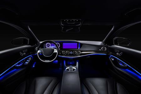
- Automotive Standard Products

XT018 – Your best choice for Automotive Standard ProductsDesigners of automotive standard products need a robust high-voltage process technology that can fulfill automotive AEC-Q100 Grade 0 requirements and has complementary low-R(ds)on high-voltage devices while enabling a very compact die size.
The entire XT018 platform is fully qualified for an extended temperature range from -40˚C to +175˚C, which enables automotive AEC-Q100 Grade 0 products. All primitive devices have also been fully modeled and characterized over the complete temperature range.
Traditionally, the 12 V board net has been adopted for passenger cars, while 24 V is often used for trucks. In addition, the new 48 V board net standard is slowly being introduced. XT018 offers a range of dedicated complementary high-voltage primitive devices that effectively cover the whole spectrum of requirements. These also deliver low R(ds)on figures, combined with robust safe-operating areas for R(ds)on, Idsat and Vt.
With its SOI/DTI isolation, XT018 allows for a more compact layout compared to bulk processes. The tight DTI spacing enables significant area savings. No complicated biased single or double HV guard rings are required. Simplified circuit layout is often possible by taking full advantage of the BCD-on-SOI benefits. A smaller die size might also open up the opportunity to select a more compact and cost-effective package.

CISSOID selected the X-FAB XT018 SOI process for its new CXT family of automotive standard products rated from -40°C to 175°C including configurable logic, voltage regulators and gate drivers. This process ideally combines high voltage and high temperature capabilities, compact layout, with automotive high quality standards.
Cissoid - The leader in high temperature semiconductors for demanding markets.
XT018 provides full PDK support for all major EDA vendors, extensive device characterization and modeling as well as a comprehensive range of analog, digital and memory IPs. Offered ESD cell libraries include low-voltage and high-voltage HBM ESD protection cells with high ESD robustness. Other powerful X-FAB design tools are the X-FAB ESD Design Checker (XESDC) and RelXplorer.
XESDC finds a set of possible ESD discharge current paths between the given chip pins of the design based on the official HBM standard. The RelXplorer is an interactive application that provides information about device and layer reliability according to application-specific mission profiles. It addresses all aspects of lifetime parameters and lifetime plots for MOS transistors, capacitors, dielectrics and interconnects.
- High-Voltage MEMS Driver ASICs

XT018 – Your best choice for High-Voltage MEMS Driver ASICsKey challenges for designers of high-voltage (HV) MEMS driver ASICs include the protection of sensitive analog and digital blocks from other “noisy” functional blocks and the availability of low-R(ds)on high-voltage primitive devices up to 200 V while pushing the layout to a compact size.
HV MEMS driver ASIC designs consist of high-voltage, digital and analog blocks. Isolating the sensitive analog and digital blocks from other functional blocks is often a challenge. Thanks to its SOI/DTI isolation, XT018 greatly enhances the noise immunity of circuits that reside in their “own separate substrate”. This feature also significantly reduces cross-talk in multi-channel implementations.
Designing HV MEMS driver ASICs requires a range of well-matched NMOS and PMOS high-voltage primitive devices. XT018 offers such high-voltage primitive devices up to 200 V, which come with low-R(ds)on performance and can be floated for high-side configurations.
With its SOI/DTI isolation, XT018 allows for a more compact layout compared to bulk processes. The tight DTI spacing enables significant area savings. No complicated biased single or double HV guard rings are required. Simplified circuit layout is often possible by taking full advantage of the BCD-on-SOI benefits.
XT018 provides full PDK support for all major EDA vendors, extensive device characterization and modeling as well as a comprehensive range of analog, digital and memory IPs. Offered ESD cell libraries include low-voltage and high-voltage HBM ESD protection cells with high ESD robustness.
Primitive devices operating at different voltage classes must be properly separated and protected. The XT018 PDK supports LVS checks for coincidence, and the DRC ensures correct spacing related to the voltage class. Dynamic Rule Distance (DRD) shows layout designers if there are any design rule issues. The provided Operating Condition Check (OCC) verifies whether all primitive devices are operating within the permitted ranges, in particular with regard to voltage limitations defined within the technology specifications.
Applications with higher operating currents are exposed to higher mechanical stress. The XT018 PowerMetal pcell supports the layout designer by reducing the effort required to draw the complex metal interconnections. The layout created by the PowerMetal pcell helps to minimize the effective mass flux in the metal interconnections. A higher stability will be reached by an ideal design.
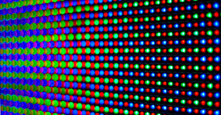
- LED Driver ICs

XT018 – Your best choice for LED Driver ICsKey challenges for designers of automotive and industrial LED driver ICs include the protection of sensitive analog and digital blocks from other “noisy” functional blocks as well as the availability of low-R(ds)on high-voltage devices while pushing the layout to a compact size.
LED driver IC designs consist of high-voltage, high-density digital and analog blocks. Isolating the sensitive analog and digital blocks from other functional blocks is often a challenge. Thanks to its SOI/DTI isolation, XT018 greatly enhances the noise immunity of circuits that reside in their “own separate substrate”. This feature also significantly reduces cross-talk in multi-channel implementations.
XT018 offers low-Rds(on) high-voltage primitive devices supporting small footprint of high-voltage driver circuits. A range of high-density capacitor options up to 6.6 fF/µm2 is also available.
With its SOI/DTI isolation, XT018 allows for a more compact layout compared to bulk processes. The tight DTI spacing enables significant area savings. No complicated biased single or double HV guard rings are required. Simplified circuit layout is often possible by taking full advantage of the BCD-on-SOI benefits, which further helps to reduce the die size.
XT018 provides full PDK support for all major EDA vendors, extensive device characterization and modeling as well as a comprehensive range of analog, digital and memory IPs. Offered ESD cell libraries include low-voltage and high-voltage HBM ESD protection cells with high ESD robustness.
Another powerful X-FAB design tool is the X-FAB ESD Design Checker (XESDC). It is a stand-alone tool that finds a set of possible ESD discharge current paths between the given chip pins of the design based on the official HBM standard. XESDC provides a first rough estimation of the HBM ESD performance early in the design phase.
XT018 comes with different NVM IP solutions for analog trimming. These include EasyFuse, TrimOTP and CEEPROM, which offer densities from 2 bit to 16 kbit. All three options are very cost-effective and do not require any additional mask layers. - Medical Power Management ICs

XT018 – Your best choice for Medical Power Management ICsKey challenges for designers of medical power management ICs include the protection of sensitive analog and digital blocks from other “noisy” functional blocks, the availability of low-R(ds)on high-voltage devices and high conversion efficiency.
Medical power management IC designs consist of high-voltage, digital and analog blocks. Isolating the sensitive analog and digital blocks from other functional blocks is often a challenge. Thanks to its SOI/DTI isolation, XT018 greatly enhances the noise immunity of circuits that reside in their “own separate substrate”.
XT018 offers a range of well-matched NMOS and PMOS high-voltage primitive devices up to 200 V. These low-Rds(on) high-voltage primitive devices have minimum high-side device impact due to the SOI/DTI process architecture.
The lack of parasitic junctions and in particular of parasitic substrate PNP bipolar transistors translates into 100% efficiency with respect to related parasitic currents. This in turn enables higher conversion efficiency and higher operating frequency.
XT018 provides full PDK support for all major EDA vendors, extensive device characterization and modeling as well as a comprehensive range of analog, digital and memory IPs. Offered ESD cell libraries include low-voltage and high-voltage HBM ESD protection cells with high ESD robustness.
Primitive devices operating in different voltage classes must be properly separated and protected. The XT018 PDK supports LVS checks for coincidence, and the DRC ensures correct spacing related to the voltage class. Dynamic Rule Distance (DRD) shows layout designers if there are any design rule issues. The provided Operating Condition Check (OCC) verifies whether all primitive devices are operating within the permitted ranges, in particular with regard to voltage limitations defined within the technology specifications.
Another powerful X-FAB design tool is the RelXplorer, an interactive application that provides information about device and layer reliability according to application-specific mission profiles. It addresses all aspects of lifetime parameters and lifetime plots for MOS transistors, capacitors, dielectrics and interconnects. - Automotive ECU Driver ICs

XT018 – Your best choice for Automotive ECU Driver ICsDesigners of automotive ECU driver ICs products need a robust high-voltage process technology that can fulfill automotive AEC-Q100 Grade 0 requirements and has complementary low-R(ds)on high-voltage devices while supporting the handling of stringent latch-up requirements.
The entire XT018 platform is fully qualified for an extended temperature range from -40˚C to +175˚C, which enables automotive AEC-Q100 Grade 0 products. All primitive devices have also been fully modeled and characterized over the complete temperature range.
XT018 offers a range of dedicated complementary high-voltage primitive devices that effectively cover the whole spectrum of automotive design requirements. These deliver low R(ds)on figures, combined with robust safe-operating areas for R(ds)on, Idsat and Vt.
Satisfying stringent latch-up requirements with bulk processes is a challenging design task. This is further aggravated by the fact that high-voltage parasitic devices are often not sufficiently modeled. With its SOI/DTI isolation, XT018 can completely eliminate latch-up, as there are no parasitic junctions between N-type and P-type devices that are placed in separate tubs.
XT018 provides full PDK support for all major EDA vendors, extensive device characterization and modeling as well as a comprehensive range of analog, digital and memory IPs. Offered ESD cell libraries include low-voltage and high-voltage HBM ESD protection cells with high ESD robustness.
The feature-rich XT018 PDK enables electromigration and IR-drop analysis as well as voltage-dependent checks. Electromigration can cause fatal long-term reliability failures. Hence, accurate, simulation-based electromigration and IR-drop analysis is advisable. X-FAB supports this through silicon-proven design reference kits.
Another powerful X-FAB design tool is the X-FAB ESD Design Checker (XESDC). It is a stand-alone tool that finds a set of possible ESD discharge current paths between the given chip pins of the design based on the official HBM standard. XESDC provides a first rough estimation of the HBM ESD performance early in the design phase. - High-Voltage Switch Arrays

XT018 – Your best choice for High-Voltage Switch ArraysKey challenges for designers of high-voltage switch arrays include the availability of complementary low-Rds(on) high-voltage devices, fast and efficient switching and reduced cross-talk while maintaining a compact layout size.
XT018 offers a range of well-matched NMOS and PMOS high-voltage primitive devices up to 200 V. These low-Rds(on) high-voltage primitive devices have minimum high-side device impact due to the SOI/DTI process architecture. This process architecture also significantly reduces cross-talk in high-voltage multi-channel implementations in a very area-efficient way.
The lack of parasitic junctions and in particular of parasitic substrate PNP bipolar transistors translates into 100% efficiency with respect to related parasitic currents. This in turn enables higher switching efficiency and operating frequency.
With its SOI/DTI isolation, XT018 allows for a more compact layout compared to bulk processes. The tight DTI spacing enables significant area savings. No complicated biased single or double HV guard rings are required. Simplified circuit layout is often possible by taking full advantage of the BCD-on-SOI benefits.
XT018 provides full PDK support for all major EDA vendors, extensive device characterization and modeling as well as a comprehensive range of analog, digital and memory IPs. Offered ESD cell libraries include low-voltage and high-voltage HBM ESD protection cells with high ESD robustness.
Primitive devices operating in different voltage classes must be properly separated and protected. The XT018 PDK supports LVS checks for coincidence, and the DRC ensures correct spacing related to the voltage class. Dynamic Rule Distance (DRD) shows layout designers if there are any design rule issues. The provided Operating Condition Check (OCC) verifies whether all primitive devices are operating within the permitted ranges, in particular with regard to voltage limitations defined within the technology specifications.
Applications with higher operating currents are exposed to higher mechanical stress. The XT018 PowerMetal pcell supports the layout designer by reducing the effort required to draw the complex metal interconnections. The layout created by the PowerMetal pcell helps to minimize the effective mass flux in the metal interconnections. A higher stability will be reached by an ideal design.
. - Smart Motor Driver ICs
XT018 – Your best choice for Smart Motor Drivers ICsKey challenges for designers of smart motor driver IC products include shielding sensitive analog and digital blocks from other “noisy” functional blocks and handling stringent latch-up requirements. In addition, complementary low-R(ds)on high-voltage devices that fulfill automotive AEC-Q100 Grade 0 requirements are needed.
Isolating sensitive analog and digital blocks from other functional blocks is often a challenge in bulk/BCD technologies. Thanks to its SOI/DTI isolation, XT018 greatly enhances the noise immunity of circuits that reside in their “own separate substrate”. Any noise on the driver output and supply pins can be effectively contained.
Satisfying stringent latch-up requirements with bulk processes is another challenging design task. This is further aggravated by the fact that high-voltage parasitic devices are often not sufficiently modeled. With its SOI/DTI isolation, XT018 can completely eliminate latch-up, as there are no parasitic junctions between N-type and P-type devices that are placed in separate tubs.
Finally, XT018 offers a range of dedicated complementary high-voltage primitive devices that effectively cover the whole spectrum of automotive motor driver design requirements. These deliver low R(ds)on figures, combined with robust safe-operating areas for R(ds)on, Idsat and Vt. The entire XT018 platform is fully qualified for an extended temperature range from -40˚C to +175˚C, which enables automotive AEC-Q100 Grade 0 products. All primitive devices have also been fully modeled and characterized over the complete temperature range.
XT018 provides full PDK support for all major EDA vendors, extensive device characterization and modeling as well as a comprehensive range of analog, digital and memory IPs. Offered ESD cell libraries include low-voltage and high-voltage HBM ESD protection cells with high ESD robustness.
X-FAB offers Silicon Frontline R3D support for XT018. This is a powerful resistive 3D extraction and analysis tool intended to improve the metallization of large power devices. Optimizing the resistance of the metal interconnect brings enormous benefits by improving efficiency through reduced losses, reduced temperature and extended reliability.
To support smart products with embedded controllers, XT018 comes with high-reliability automotive Flash IP designed for operation in harsh conditions. The high-volume production proven memory is AEC-Q100 Grade 0 compliant, featuring an extended temperature range from -40˚C to +175˚C.
- Ultra-Low Power IoT Sensor Interface ICs

XT018 – Your best choice for Ultra-Low Power IoT Sensor Interface ICsKey challenges for designers of ultra-low power (ULP) IoT sensor interface ICs are isolating precision analog circuits from other noisier parts of the IC and managing the ULP requirements while pushing the layout to a compact size.
ULP IoT sensor interface IC designs consist of sensitive analog, digital and memory blocks. Effective SoC area partitioning becomes even more important if the design includes power-gating features to put parts of the circuit into a deep sleep state in order to save power. Thanks to its SOI/DTI isolation, XT018 greatly enhances the noise immunity of circuits that reside in their “own separate substrate”. Another aspect of the BCD-on-SOI process architecture is that it reduces junction leakage especially at elevated temperatures.
The lack of parasitic junctions and in particular of parasitic substrate PNP bipolar transistors translates into 100% efficiency with respect to related parasitic currents. This in turn enables higher conversion efficiency and overall power savings.
Thanks to its SOI/DTI isolation, XT018 allows for a more compact layout compared to bulk processes. The tight DTI spacing enables significant area savings. No complicated biased single or double HV guard rings are required. Simplified circuit layout is often possible by taking full advantage of the BCD-on-SOI benefits.
XT018 provides full PDK support for all major EDA vendors, extensive device characterization and modeling as well as a comprehensive range of analog, digital and memory IPs. Offered ESD cell libraries include low-voltage and high-voltage HBM ESD protection cells with high ESD robustness.
Digital performance is mainly determined by the speed of the switching edges, which in turn depends on the threshold voltage. XT018 comes with a number of compatible multi-Vt standard cell libraries, which provide additional flexibility for designers to balance the power and speed of their digital blocks. This also includes a special near-threshold voltage library.
Accurate SPICE models are an essential ingredient for good circuit designs, enabling designers to check the integrity of their designs and predict circuit behavior. X-FAB is proud to provide best-in-class models with focus on analog devices that come with superior model quality and matching models to enable first-time-right designs. - Universal Gate Driver ICs

XT018 – Your best choice for Universal Gate Driver ICsKey challenges for designers of universal gate driver ICs include the availability of complementary low-Rds(on) high-voltage devices that can be floated for high-side operation, the handling of stringent latch-up requirements as well as fast and efficient switching.
XT018 offers a range of high-voltage primitive devices that can be freely floated up to 400 V. These low-Rds(on) high-voltage primitive devices have minimum high-side device impact due to the SOI/DTI process architecture. This process architecture also significantly reduces cross-talk in high-voltage multi-channel implementations in a very area-efficient way.
Universal gate driver ICs need to fulfill stringent latch-up requirements. Satisfying these with bulk processes is a challenging design task. This is further aggravated by the fact that high-voltage parasitic devices are often not sufficiently modeled. With its SOI/DTI isolation, XT018 can completely eliminate latch-up, as there are no parasitic junctions between N-type and P-type devices that are placed in separate tubs.
The lack of parasitic junctions and in particular of parasitic substrate PNP bipolar transistors also translates into 100% efficiency with respect to related parasitic currents. This in turn enables higher switching efficiency and operating frequency.
XT018 provides full PDK support for all major EDA vendors, extensive device characterization and modeling as well as a comprehensive range of analog, digital and memory IPs. Offered ESD cell libraries include low-voltage and high-voltage HBM ESD protection cells with high ESD robustness.
X-FAB offers Silicon Frontline R3D support for XT018. This is a powerful resistive 3D extraction and analysis tool intended to improve the metallization of large power devices. Optimizing the resistance of the metal interconnect brings enormous benefits by improving efficiency through reduced losses, reduced temperature and extended reliability.
Another powerful X-FAB design tool is the RelXplorer, an interactive application that provides information about device and layer reliability according to application-specific mission profiles. It addresses all aspects of lifetime parameters and lifetime plots for MOS transistors, capacitors, dielectrics and interconnects.
- Pixel Array Sensor Interface ICs
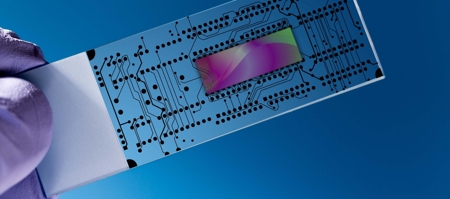
XT018 – Your best choice for Pixel Array Sensor Interface ICsKey challenges for designers of pixel array sensor interface ICs include the availability of low-R(ds)on high-voltage devices, isolating the sensitive analog and digital blocks of each pixel from each other and maximizing the usable circuit area available for each pixel.
XT018 offers a range of well-matched NMOS and PMOS high-voltage primitive devices up to 375 V. These low-R(ds)on high-voltage primitive devices have minimum high-side device impact due to the SOI/DTI process architecture.
Pixel array sensor interface IC designs consist of numerous small circuit blocks comprising high-voltage, digital and analog components. Isolating these sensitive blocks from other each other is often a challenge. Thanks to its SOI/DTI isolation, XT018 greatly enhances the noise immunity of circuits that reside in their “own separate substrate”.
For the same reason, XT018 allows for a much more compact layout compared to bulk processes. The tight DTI spacing enables significant area savings. No complicated biased single or double HV guard rings are required.
XT018 provides full PDK support for all major EDA vendors, extensive device characterization and modeling as well as a comprehensive range of analog, digital and memory IPs. Offered ESD cell libraries include low-voltage and high-voltage HBM ESD protection cells with high ESD robustness.
Accurate SPICE models are an essential ingredient for good circuit designs, enabling designers to check the integrity of their designs and predict circuit behavior. X-FAB is proud to provide best-in-class models with focus on analog devices that come with superior model quality and matching models to enable first-time-right designs.
XT018 comes with different NVM IP solutions for analog trimming. These include EasyFuse, TrimOTP and CEEPROM, which offer densities from 2 bit to 16 kbit. All three options are very cost-effective and do not require any additional mask layers. - Line-Powered IoT Edge ICs

XT018 – Your best choice for Line-Powered IoT Edge ICsKey challenges for designers of line-powered IoT edge ICs include the availability of complementary low-Rds(on) high-voltage devices and the protection of sensitive analog and digital blocks from other “noisy” functional blocks. Achieving the smallest die size without compromising product features or performance is another critical aspect.
Line-powered IoT edge IC designs require high-voltage primitive devices with an operating voltage of 375 V to support line voltages up to 265 V AC. XT018 offers such complementary high-voltage primitive devices. In addition, there is a range of other high-voltage devices that can be floated up to 400 V above the handle wafer potential.
Isolating the sensitive analog and digital blocks from the high-voltage AC-DC converter section is a challenge. With its SOI/DTI isolation, this can easily be implemented in XT018, which also greatly enhances the noise immunity of circuits that reside in their “own separate substrate”. Multi-channel implementations become much easier to realize with this feature as well.
In addition, the SOI/DTI isolation of XT018 allows for a more compact layout compared to bulk processes. The tight DTI spacing enables significant area savings. No complicated biased single or double HV guard rings are required. Simplified circuit layout is often possible by taking full advantage of the BCD-on-SOI benefits.
XT018 provides full PDK support for all major EDA vendors, extensive device characterization and modeling as well as a comprehensive range of analog, digital and memory IPs. Offered ESD cell libraries include low-voltage and high-voltage HBM ESD protection cells with high ESD robustness.
Applications with higher operating currents are exposed to higher mechanical stress. The XT018 PowerMetal pcell supports the layout designer by reducing the effort required to draw the complex metal interconnections. The layout created by the PowerMetal pcell helps to minimize the effective mass flux in the metal interconnections. A higher stability will be reached by an ideal design.
Primitive devices operating in different voltage classes must be properly separated and protected. The XT018 PDK supports LVS checks for coincidence, and the DRC ensures correct spacing related to the voltage class. Dynamic Rule Distance (DRD) shows layout designers if there are any design rule issues. The provided Operating Condition Check (OCC) verifies whether all primitive devices are operating within the permitted ranges, in particular with regard to voltage limitations defined within the technology specifications.
- Aerospace ASICs

XT018 – Your best choice for Aerospace ASICsDesigners of aerospace ASICs require a robust high-voltage process technology that can support the handling of negative transients and enables effective shielding of sensitive analog and digital blocks from other “noisy” functional blocks.
XT018 offers a range of well-matched NMOS and PMOS high-voltage primitive devices up to 375 V. These deliver low R(ds)on figures combined with robust safe-operating areas for R(ds)on, Idsat and Vt and have minimum high-side device impact due to the SOI/DTI process architecture.
Aerospace ASICs have to function reliably in very harsh environments. This also means that these ICs need to incorporate effective protection against over-voltages and negative transients. Thanks to its SOI/DTI architecture, XT018 greatly simplifies the implementation of such protection. In addition, X-FAB provides an extensive ESD cell library, which includes special latch-up-robust ESD clamps suitable for reverse voltages. With these benefits, XT018 effectively enables first-time-right designs.
Isolating sensitive analog and digital blocks from other functional blocks is often a challenge. With its SOI/DTI isolation, XT018 greatly enhances the noise immunity of circuits that reside in their “own separate substrate”. Multi-channel implementations also become much easier to realize with this feature, which effectively reduces cross-talk.
XT018 provides full PDK support for all major EDA vendors, extensive device characterization and modeling as well as a comprehensive range of analog, digital and memory IPs. Other powerful X-FAB design tools are the X-FAB ESD Design Checker (XESDC) and RelXplorer.
XESDC finds a set of possible ESD discharge current paths between the given chip pins of the design based on the official HBM standard. The RelXplorer is an interactive application that provides information about device and layer reliability according to application-specific mission profiles. It addresses all aspects of lifetime parameters and lifetime plots for MOS transistors, capacitors, dielectrics and interconnects.


Contact

Tilman Metzger
Technical Marketing Manager
High Voltage
tilman.metzger@xfab.com
For more information, please contact us: