RF and Wireless
In today’s connected world, radio frequency (RF) electromagnetic signals are key for enabling many everyday tasks. Making a phone call or browsing the Internet with your smartphone at home or on the street is only possible with RF signals. Likewise, it is thanks to RF signals that you can find the right direction to your destination with your car’s on-board GPS device.
RF signals are used not only for human–machine interfaces, but also for machine-to-machine communication. As wireless means of communication, they enable more flexibility and scalability without overloading existing infrastructures with cables or wires.
To satisfy the corresponding demand, we offer RF solutions for various applications, such as:
- Cellular standards: 2G, 3G, 4G (LTE) and now 5G NR
- WLAN connectivity: up to 802.11ax, Wi-Fi 6
- Short and medium range communication, such as Bluetooth
- Positioning: GPS, Galileo, BeiDou or GLONASS
- Vehicle-to-everything communication (V2x)
- Internet of Things (IoT): RFID and low-power networks, such as LoRa or Sigfox
Around 25% of the smartphones shipped worldwide contain a chip produced by X-FAB.
Areas of expertise


Solutions
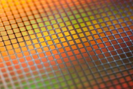
RF SOI platform – XR013
XR013 is our 130 nm modular, feature-rich RF SOI technology solution suitable for multiple air interface standards and both fixed and mobile applications, such as smartphones, infrastructure and WLAN connectivity devices. The high isolation and low insertion losses make XR013 a good fit for RF switching applications in front-end modules for 2G, 3G, 4G LTE Advanced and 5G New Radio designs. Low-noise amplifiers demonstrating low noise figure, high gain and high linearity thanks to NFET options complete our XR013 RF SOI offer.
Standard features include a twin-well 2.5 V CMOS technology on a linear, high-impedance SOI substrate with four levels of metal in a hybrid copper and aluminum metallization that supports wire bond, bump, or Cu pillar chip–package interfaces and a large array of passive analog RF devices.
Optional features include a range of FET devices such as multiple threshold voltage (Vt) options, up to two additional digital routings and up to two additional thick copper metal levels.
The technology offers a comprehensive set of components supported by Si-proven, advanced RF models. In addition, as design enablers, we have created and provide a wide range of IP blocks.
With economy of scale advantages and opportunities for further innovative RF integration, XR013 deliver both performance and cost advantages.
All in all, our XR013 platform offers flexibility to customize and create cost-effective configurations with few mutually exclusive features.
Key features:
- Low RonCoff figure of merit for RF switches with surface-potential-based (PSP) compact models, including advanced modelization of a high-impedance SOI substrate
- Low-noise, high-gain, high-linearity NFET options for RF switch and low-noise amplifier integration
- 2.5 V CMOS platform with hybrid Cu/Al metallization with optional thick Cu levels
- Both low- and high-value diffusion and poly resistors including a 3 kΩ/sq p-poly resistor
- High-density vertical RF metal–insulator–metal (MIM) capacitor and vertical parallel plate capacitors (VPP)
- Large catalog of high-Q, symmetric, octagonal inductors for multiple metallization configurations
- 1.2 V- and 2.5 V-based RF varactors
- Optional low-leakage 1.2 V CMOS module
- Si-proven RF reference kits
- Si-proven analog and digital IP
- Si-proven I-fuse OTP memory IP by Attopsemi
- Si-proven eFuse and supporting IP
- Si-proven general-purpose input/output (GPIO) libraries including electrostatic discharge (ESD) solutions
- Comprehensive PDK support for Cadence, Siemens EDA and Keysight ADS with Electromagnetic simulations possible with Cadence EMX, Keysight Momentum & RFpro and Ansys HFSS
RF CMOS
350 nm high-temperature modular mixed-signal technology
The XA035 series is our 350 nm high-temperature CMOS technology. While being best suited for high-temperature automotive and industrial products with operating temperatures of up to 175°C, XA035 is also targeted at medical and avionic markets. All modules are comparable in design rules and transistor performance with our corporate state-of-the-art 350 nm CMOS processes.
Comprehensive design rules, precise SPICE models, analog and digital libraries, IPs and development kits support the process on platforms supplied by the major EDA tool vendors.Key features:
- 3.3 V logic layout & performance compatible with XH035 and the industry standard
- 350 nm single poly, triple metal N-well CMOS basic process
- Extended high temperature characterization, up to 175°C operating temperature, beyond AEC-Q100 requirement
- Improved ESD robust devices
- Very high resistivity poly resistor module
- Double poly Capacitor module
- Single and double metal-insulator-metal (MIM) capacitors
- Isolated MOS module
- Mid and thick gate oxide modules for high-voltage transistors
- Depletion NMOS module
- Buried N module
- Tiny EEPROM or core EEPROM modules
- Flat passivation module
- Polyimide module
- Thick top metal-3 or metal-4 modules
- Lifetime Calculator tool for device reliability estimation based on automotive mission profile
- Input/output cell library with 4 kV human body model ESD protection levels
- RF characterization and models for all RF MOS transistors and passive components
- Comprehensive PDK support for Cadence, Siemens EDA, Synopsys and others
350 nm modular mixed-signal technology with high-voltage extensions
The XH035 series is our 350 nm modular mixed-signal technology. Main target applications are standard cell, semi-custom and full custom designs for industrial, automotive and telecommunication products. Based on a single-poly, triple-metal 350 nm drawn gate length process for digital applications, it features core and process modules such as low-Vt, low-leakage, embedded non-volatile memory and high-voltage options, as well as standard or thick fourth layer of metal, double-poly and MIM capacitors and high-resistivity polysilicon. MOS and bipolar transistors are also available. World-class low-noise PMOS and NMOS transistors make this technology the first choice for applications requiring very low noise and high signal-to-noise ratios. A suite of RF active and passive components is also available.
DMOS transistors are available for multiple operating voltages up to 100 V. The 45 V DMOS transistors come with a 45% lower on-resistance, which can reduce the chip area by up to 40%, resulting in significant cost savings.
The 3.3 V CMOS cores are compatible in design rules and transistor performance with state-of-the-art 350 nm CMOS processes.Key features:
- Standard, low threshold or low leakage 3.3 V or standard 5 V core module
- 350 nm single poly, triple metal CMOS basic process with modular concept (1P3M)
- 5 V dual gate or 5 V only module
- Four layers metal options for high density circuits
- Thick top metal for inductors and Smart Power applications
- Low noise and medium voltage PMOS and NMOS transistors
- Compact high-voltage devices
- Isolated MOS module
- Mid and thick gate oxide modules for high-voltage transistors
- Depletion NMOS module
- Buried N module
- Core module EEPROM, tiny EEPROM, programmable polyfuse
- Very high resistivity poly resistor module
- Single, double metal-insulator-metal (MIM) capacitors
- Stacked MIM and poly-insulator-poly (PIP) capacitors with high capacitance area
- Thick top metal-3 or metal-4 modules
- Special opto modules to increase optical sensitivity and reduce dark current
- Photodiode module
- Pixel module
- Integrated MEMS Pressure Sensors module.
- Polyimide module for stress relief & passivation protection
- Input/output cell library with 4 kV human body model ESD protection levels
- Comprehensive PDK support for Cadence, Siemens EDA, Synopsys and others
350 nm modular CMOS technology for fast optical applications
XO035 is our specialized process for optoelectronic and high-speed RF applications. It is especially suited for applications needing sensitive high-bandwidth photodiode arrays or CMOS image sensors, such as optical data storage, optical data communication or high dynamic range cameras.
In addition to the single-poly, triple-metal 350 nm drawn gate length process for digital applications, process modules are available for 5 V drain source and isolated transistors, double-poly and MIM capacitors and high-resistivity poly resistors.
Special optoelectronic process modules allow an optimized PIN cathode implantation, optical window etching and dedicated antireflective coating (ARC) layer deposition. Bipolar and MOS Transistors are available so is a suite of RF active and passive components. A highly sensitive PIN diode supports wavelengths from 400nm to 900nm, optimized for maximum quantum efficiency at blue light.Key features:
- 3.3 V logic layout & performance compatible with the industry standard
- 350 nm single poly, triple metal, N-well CMOS basic process (1P3M)
- High bandwidth, high sensitivity PIN diode
- Modular concept
- 5 V dual gate module
- Single and double metal-insulator-metal (MIM) capacitors for RF and high linear applications
- High resistivity poly resistor module
- Well isolated 3.3 V and 5 V devices
- Mid gate oxide (5 V) module
- Diode and MOS varactors
- Four layers metal options for high density circuits
- Competitive RF performance
- Optical module
- Input/output cell library with 4kV HBM ESD protection levels
- Diva, Dracula, Assura, Calibre, Hercules DRC & LVS and parasitic extraction
- RF characterization and models for all RF MOS transistors and passive components
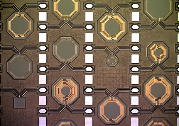
XIPD – RF Integrated Passive Devices
The XIPD is X-FAB’s modular High-Resistivity Silicon passive technology suitable for high RF performance Integrated Passive Devices (inductors, capacitors and resistors) required in multiple air interface standards, including 5G mmW or coming 6G, operating in the temperature range of -40 to 125°C. Standard features include engineered high-impedance Si substrate with 3 levels of metal in a hybrid thick copper and aluminum metallization that supports wire-bond, bump, or Cu-pillar chip-package interfaces and a large array of passive analog RF devices. Optional feature includes 1 additional thick Cu metal level.
Globally, the platform offers flexibility to customize and create cost effective & high-performance configurations with few mutually exclusive features. XIPD offers a full PDK support for major EDA vendors, comprehensive set of components supported by Si-proven, advanced RF models.
Through use of the XIPD platform, demands for more compact RF/EMI filtering, matching networks, baluns and couplers can be met via the fabrication of fully integrated high-quality passive components with improved performance characteristics.
Key Features:
- Large catalog of high-Q, symmetric, octagonal inductors for multiple metallization configurations
- Thick Cu levels provide a high-performance pathway to minimize system losses
- 2.1 fF/ µm2 vertical RF Metal-Insulator-Metal capacitor
- Comprehensive PDK support for Cadence, Siemens EDA and Keysight ADS
- Electromagnetic simulations possible with Cadence EMX, Keysight Momentum & RFpro
BiCMOS
XB06 – 0.60 µm modular CMOS technology
The XB06 series is our 0.60 µm BiCMOS technology. Main target applications are RF circuits and high-precision analog applications mixed with digital parts for telecommunication, consumer, automotive and industrial products. The digital part is fully compatible with the CX06 0.60 µm process family. Reliable design rules, precise SPICE models, digital libraries and analog IP together with support for all major EDA tools provide an efficient chip design ecosystem.
Key features:
- 0.60 µm double poly, double metal N-well CMOS process
- Standard CMOS Core Module (2P2M)
- PIN diode with improved sensitivity (at 405 nm) for high-speed optical applications
- Junction FET transistor, light shield and polyimide module
- Natural PMOS module for PIN module
- Circular n-channel junction FET transistor
- Schottky diode with improved forward characteristics
- 5 V and 3.3 V cell libraries
- HV depletion transistor
- No-burried-layer-doping module
- Optoelectronic integrated circuit and RF cells libraries
- High frequency NPN transistor with poly emitter and buried collector
- 0.5 µm bipolar module
- Large number of bipolar primitive devices
- Varicap diode module
- Double poly capacitor module with high capacity per area
- Single metal-insulator-metal (MIM) capacitors for RF and high linear applications
- High resistivity poly resistor module
- MOS varactor & third metal layer
- Special inductors in third thick metal
- Optical window module
- Electrostatic discharge (ESD) protection in accordance with MIL-STD
- High-density RAM, DPRAM, ROM blocks
- OTP options: zener-zaps and poly fuses
- EPROM option
Applications
- Cellular handsets and tablets
Cellular handsets and tablets supporting cellular air standards from 2G to 5G New Radio (Sub-6 GHz) require numerous RF components between the modem IC and the antennas, called the RF front-end. For these RF front-ends, our RF technologies enable high-performance RF switches, low-noise amplifiers and antenna tuners.
The key parameters of such RF components are low insertion losses (low Ron) and high isolation (low Coff) together with high linearity. These parameters translate into battery savings and long communication range for the end product.

- WLAN connectivity
The Wi-Fi standard has become part of our everyday lives at home, at work, on the road – everywhere. The latest Wi-Fi 6 standard brings enhanced broadband connection to users’ smartphones and set-top boxes, as well as higher capacity to customer-premises equipment and access points. These use cases are made possible by our RF technologies for WLAN front-ends.
RF switches and low-noise amplifiers based on our RF SOI or RF CMOS process are among the key components making up WLAN RF front-ends that allow you to share the smartphone content on a Smart TV, for instance.

- Base stations and small cells
Small cells bring a significant network coverage improvement for 4G and 5G standards, but also for legacy standards (2G and 3G). In addition to small cells, 5G macro cells or massive MIMO (mMIMO) are also used to improve network coverage.
Due to the lower power level requirements of small cells, our RF SOI technology is a perfect candidate for the necessary RF front-end components. In remote radio head and active antenna systems for 5G mMIMO macro cells, our XR013-based RF switches and low-noise amplifiers provide attractive RF performance to ensure a reliable communication link.

- V2X communication
Reducing road fatalities is a common goal of all automotive players worldwide. In this context, vehicle-to-everything (V2X) communication based on either the cellular (LTE/5G PC5) or Wi-Fi (802.11p) standard plays an essential part in efforts to reduce the number of car accidents.
As an extension of the solutions we provide for cellular handsets and WLAN connectivity, our RF SOI or BiCMOS technologies enable the design of key RF front-end components that make highly reliable, low-latency communication between vehicles possible.

- IoT devices
Smartphones and computers are not the only devices connected to a network. Internet of Things (IoT) devices use various wireless standards (Sigfox, LoRa, etc.), but need to meet mainly one requirement: low-power communication.
Our RF CMOS technology provides cost effective one chip solution for an IoT transceiver whereas our RF SOI process combines both low power consumption and good RF performances.
The intrinsic advantages of the SOI technology such as low power supply voltage and low capacitance, can also be leveraged, for instance, for the digital integration in RFID transceiver chips.


Related Resources
Contact

David Auffret
Technical Marketing Manager
RF
For more information, please contact us: