Stable and diversified manufacturing

Our Fabs

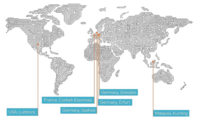
As a global foundry group, X-FAB provides a comprehensive set of specialty technologies and design IP enabling its customers to develop world-leading semiconductor products that are manufactured at X-FAB's six wafer fabs located in Malaysia, Germany, France, and the United States. With its expertise in analog/mixed-signal technologies, microsystems/MEMS and silicon carbide (SiC), X-FAB is the development and manufacturing partner for its customers, primarily serving the automotive, industrial and medical end markets.
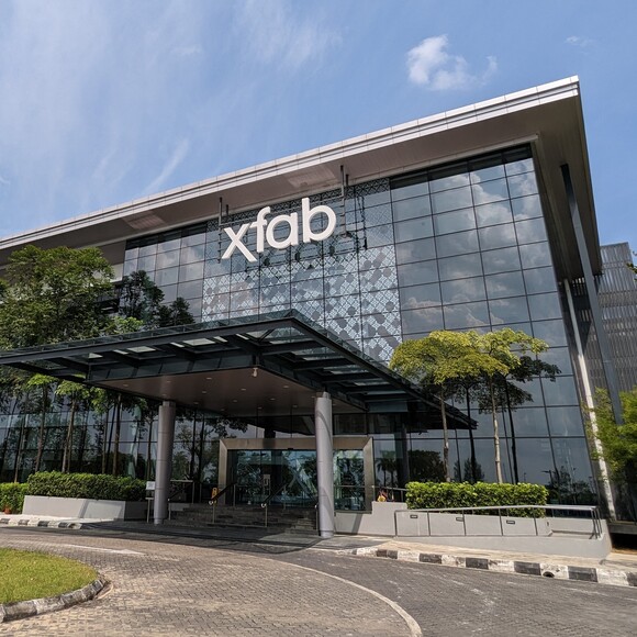
Kuching, Sarawak (Malaysia)
Processes:

  • 350 nm, 180 nm and 130 nm CMOS logic and mixed-signal
  • 350 nm, 180 nm high voltage
  • 180 nm BCD-on-SOI

Clean room class:

  • 10 and 100 (8" with SMIF)

Contact details:

X-FAB Sarawak Sdn. Bhd.
1, Silicon Drive, Sama Jaya Free Ind. Zone,
93350 Kuching, Sarawak, Malaysia

Tel.: +60 82-354 888
Fax: +60 82-363 330

Welcome to X-FAB Sarawak

Take a tour of the site and learn more about the challenging projects, groundbreaking developments and working environment. Our colleagues will show you around the manufacturing and administrative areas, and the site CEO will tell you more about our ongoing expansion program.

Watch Video

Take a tour of the site

Explore our semiconductor facility in Kuching, Malaysia by taking a virtual tour of the office area, cafeteria, and clean room manufacturing.

Virtual Tour

Watch Video

Erfurt, Germany

Processes:

  • modular 1.0 µm CMOS mixed-signal processes (analog, high voltage and EEPROM)
  • 2 and 3 layer metal
  • special micromechanical sensor processes (MEMS)
  • special smart power options
  • special SOI process options

Clean room class:

  • 1 and 10

Contact details:

X-FAB Semiconductor Foundries GmbH
Haarbergstr. 67
99097 Erfurt, Germany
Tel.: +49 361-427 6000
Fax: +49 361-427 6111

Dresden, Germany

Processes:

  • 350 nm analog/mixed-signal CMOS process (XH035)
  • special purpose customer specific 1.0 µm and 350 nm analog/mixed-signal CMOS processes

Clean room class:

  • 1

Contact details:

X-FAB Dresden GmbH & Co. KG
Grenzstrasse 28
01109 Dresden
Germany

Tel.: +49 351 4075 6 0
Fax: +49 351 4075 6 418

Take a tour of the site

Explore our semiconductor facility in Dresden, Germany by taking a virtual tour of the office area, cafeteria, and clean room manufacturing.

read more

Itzehoe, Germany

Process / technical capabilities:

  • Physical sensors: acceleration, angular rate, mass flow
  • MOEMS: micro mirror scanner, microoptics 
  • RF-MEMS: variable capacity RF switches
  • Novel technology development: piezoelectric MEMS actuators
  • Wafer level packaging: AuSi, AuSn, glass frit, anodic, Getter integration, TSV

Contact details:

X-FAB MEMS Foundry Itzehoe GmbH
Fraunhoferstrasse 1
25524 Itzehoe
Germany

Tel.: +49 4821 956 4700
Fax: +49 4821 956 4999

Corbeil-Essonnes, France

Processes:

  • 110 nm BCD-on-SOI process
  • 130 nm RF-SOI processes
  • 180 nm analog/mixed-signal CMOS process
  • 180 nm BCD-on-SOI process

Clean room class:

  • 1

Contact details:

X-FAB France SAS
224 Boulevard John Kennedy
91105 Corbeil-Essonnes Cedex
France

Tel.: +33 1 60 88 51 51

Lubbock, Texas (USA)

Processes:

  • modular 1.0 µm CMOS mixed signal process
    (high voltage, EEPROM, low voltage)
  • modular 0.8 µm mixed-signal processes
    (high voltage, CMOS, BiCMOS)
  • a range of SiC processing capabilities 

Clean room class:

  • 10

Contact details:

X-FAB Texas, Inc.
2301 N. University Ave.
Lubbock, TX 79415, USA

Tel.: +1 806-747-4400 Ext. 2271
Fax: +1 806-747-3111

Contact

For more information, please contact us:

By submitting the form you agree to our privacy policy.
Fields marked with “*” are mandatory