High-Voltage
X-FAB has an unparalleled foundry track record in supporting high-voltage (HV) applications across all major segments (automotive, industrial, medical, communication and consumer). We offer a broad portfolio of highly modular high-voltage solutions.
Advantages:
- Robust and reliable with best-in-class Rds(on)
- Supporting automotive AEC-Q100 Grade 0
- Embedded non-volatile memory (NVM) options including EEPROM and Flash
- Comprehensive portfolio ranging from 1 um (6-inch wafers) to 180 nm (8-inch wafers)
High Voltage devices power more than 60% of our business.
Our broad portfolio of highly modular high-voltage solutions
1 µm | 0.60 µm | 350 nm | 180 nm | 110 nm | |
|---|---|---|---|---|---|
625 V / 650 V |
|
|
|
| |
340 V / 400 V |
|
|
|
| |
200 V / 290 V |
|
|
|
| |
125 V / 155 V |
|
|
|
| |
90 V / 100 V |
|
|
|
| |
55 V / 60 V |
|
|
|
|
|
40 V / 45 V |
|
|
|
|
|
30V / 32 V |
|
|
|
| |
20 V / 25 V |
|
|
|
| |
12 V / 15 V |
|
|
|
|
|

FeatureXplorer - Your access to our technology portfolio
Get a quick overview of our broad technology portfolio in our FeatureXplorer. Here you are able to select the right foundry process for your next chip design.
Areas of expertise
As the specialty foundry for the analog world, we gained an unparalleled breadth of know-how and experience in the high-voltage area. Our first BCD-on-SOI process was developed more than 25 years ago. With introduction of our galvanic isolation solution in 2018, we entered a new area of ultra-high-voltage expertise far beyond conventional CMOS technologies that supports up to 650 V. We now offer one of the broadest portfolios of high-voltage solutions in the foundry world.
BCD-on-SOI
X-FAB is the foundry leader in BCD-on-SOI solutions. We provide the most extensive HV SOI technology offering ranging from 1 µm to 180 nm, supporting automotive AEC-Q100 Grade 0 and voltages up to 100 V.
HV CMOS
We offer a comprehensive HV CMOS technology portfolio ranging from 1 µm to 180 nm, supporting automotive AEC-Q100 Grade 0 and voltages up to 650 V.
Galvanic Isolation
Our galvanic isolation technology achieves best-in-class isolation performance and enables both capacitive and inductive coupler implementations. It supports automotive AEC-Q100 Grade 0.
Solutions
BCD-on-SOI
X-FAB offers the most extensive foundry BCD-on-SOI technology portfolio. Our modular solutions combine the benefits of SOI wafers with deep trench isolation (DTI) and a wide range of robust HV CMOS, bipolar and well-matched passive primitive devices.
Key benefits of our BCD-on-SOI solutions are:
- Reduced isolation distances
- No parasitic bipolar effects to substrate, latch-up can be completely eliminated
- Excellent EMI and EMC robustness
- Simplifies handling of below-ground supply voltages and negative transients
- Compact implementation of voltage stacking while greatly reducing cross-talk
- Support of complex integration of high-density logic with HV and analog devices, including floating high-side configurations
- Low junction leakage at high temperatures
- Faster time-to-market (fewer redesigns)
Automotive 110nm BCD-on-SOI Technology Platform
XT011 is X-FAB’s next generation BCD-on-SOI technology. It combines the benefit of SOI wafers with Deep Trench Isolation (DTI) and those of a state-of-the-art 110 nm process. It offers more than twice the standard cell library density compared to XT018.
XT011 features multile high voltage options and a range of automotive Grade-0 non-volatile memory options. The XT011 platform is specifically designed for a next generation automotive, industrial and medical applications operating in the temperature range of -40°C to 175°C. Full PDK support for major EDA vendors, extensive device characterization and modeling, comprehensive set of digital and memory IPs.Key features:
- Fully modular 110nm SOI process based on low mask count 5V Single Gate core module
- Up to eight metal layers with different thick metal options
- Deep Trench Isolation
- Up to 175ºC operating temperature supporting AEC-Q100 Grade 0
- Unique integration of digital, analog, HV, NVM and SOI in a single process
- High-reliability automotive NVM solutions including Flash
- 12V - 60V HV CMOS transistors
- Excellent specific Ron HV N-channel device performance
- Metal Fringe capacitors
- Comprehensive PDK support for Cadence, Mentor, Synopsys and Tanner
Automotive 180 nm BCD-on-SOI technology platform
XT018 is X-FAB’s premier 180 nm modular high-voltage BCD-on-SOI technology. It combines the benefit of SOI wafers with Deep Trench Isolation (DTI) and those of a state-of-the-art six metal layers 180 nm process. XT018 features a complete portfolio of voltage options from 10 V to 375 V as well as a full range of automotive grade-0 qualified non-volatile memory options.
The XT018 platform is specifically designed for a next generation automotive, industrial and medical applications operating in the temperature range of -40 to 175°C.
Best-in-class PDK support for all major EDA vendors, extensive device characterization and modeling, comprehensive set of analog, digital, and memory IPs.Key features:
- Fully modular 180 nm SOI process based on low mask count 5 V Single Gate core module
- Up to six metal layers with different thick metal options
- Deep Trench Isolation and Handle Wafer Contact
- Up to 175ºC operating temperature supporting AEC-Q100 Grade 0
- Unique integration of digital, analog, HV, NVM and SOI in a single process
- High-reliability automotive NVM solutions including embedded Flash, EEPROM and OTP
- 10 V to 375 V high-voltage CMOS transistors
- Excellent specific Ron HV N-channel device performance
- High gain BJTs
- Very fast forward HV, Schottky and Zener diodes
- Standard and high capacitance single, double, triple MIM and metal fringe capacitors
- Comprehensive PDK support for Cadence, Siemens EDA, Synopsys and others
- Silicon Frontline R3D support for metal optimization
0.6 µm modular BCD-on-SOI technology platform
XT06 is X-FAB’s mature 0.6 µm modular high-voltage BCD-on-SOI technology. It combines the benefit of SOI wafers with Deep Trench Isolation (DTI) and a cost effective 0.6 µm process. XT06 features high-voltage primitive devices from 8 V to 60 V as well as a range of non-volatile memory options with operating temperature range of -40 to 125 °C.
Best-in-class PDK support for all major EDA vendors, extensive device characterization and modelling, comprehensive analog, digital, and memory IPs.Key features:
- Modular 0.6 µm 5 V single poly core process
- Up to 3 metal layers with thick power metal option
- 8 V, 12 V, 30 V and 60 V HV transistors with 18 V gate oxide
- 8 V and 30 V depletion devices
- Vertical PNP and NPN BJTs
- Protection, rectifier and Schottky diodes
- 60 V resistors and capacitors
- EasyFuse and EEPROM NVM IP options
- Comprehensive PDK support for Cadence, Siemens EDA, Synopsys and others
1 µm 90 V 225 ˚C SOI technology platform
XI10 is a robust dielectric trench insulated 90 V technology solution supporting up to 225 ˚C junction temperature. The 13 layers 90 V core process module provides trench insulation, single level poly and 3 level of metal.
Best-in-class PDK support for all major EDA vendors, extensive device characterization and modelling, digital and memory IPs.Key features:
- 1 µm single poly 3 metal core process
- 5 V CMOS transistors
- 40 V, 60 V and 90 V NMOS and 30 V and 40 V PMOS transistors
- High temperature Tungsten metalization option
- Comprehensive PDK support for Cadence, Siemens EDA, Synopsys and others
1 µm modular 625 V BCD-on-SOI technology platform
XDH10 is a robust dielectric trench insulated Ultra High Voltage (UHV) technology solution. The modular process provides a wide variety of passive, MOS and bipolar devices with dielectric bi-directional high voltage trench insulation. The 14 layers 625 V core process module provides trench insulation, single level poly with thick gate oxide and a third level metal with power metal.
Best-in-class PDK support for all major EDA vendors, extensive device characterization and modelling, comprehensive analog, digital, and memory IPs.Key features:
- Modular 1 µm single poly 3 metal core process
- 5 V and 7 V CMOS transistors
- 15 V, 20 V and 32 V NMOS and 20 V PMOS transistors
- Scalable UHV NDMOS & PMOS transistors
- 600 V IGBT
- High performance NPN and PNP transistors with up to 600 VCE
- 7 V and UHV depletion transistors
- Schottky and Zener diodes
- 650 V capacitor and resistor
- Comprehensive PDK support for Cadence, Siemens EDA, Synopsys and others
1 µm modular 340 V BCD-on-SOI technology platform
XDM10 is a robust dielectric trench insulated Ultra High Voltage (UHV) technology solution. The modular process provides a wide variety of passive, MOS and bipolar devices with dielectric bi-directional high voltage trench insulation. The 14 layers 340 V core process module provides trench insulation, single level poly with thick gate oxide and a third level metal with power metal.
Best-in-class PDK support for all major EDA vendors, extensive device characterization and modelling, comprehensive analog, digital, and memory IPs.Key features:
- Modular 1 µm single poly 3 metal core process
- 5 V and 7 V CMOS transistors
- 15 V, 20 V and 32 V NMOS and 20 V PMOS transistors
- Scalable UHV NDMOS & PMOS transistors
- 340 V IGBT
- High performance NPN and PNP transistors with up to 330 VCE
- 7 V and UHV depletion transistors
- Schottky and Zener diodes
- 350 V capacitor and resistor
- Comprehensive PDK support for Cadence, Siemens EDA, Synopsys and others
High-voltage CMOS solutions
X-FAB offers a wide range of fully modular HV solutions down to 180 nm. With a clear focus on automotive applications, these technologies are also successfully adopted in medical, industrial and consumer applications.
The breadth of our available modules and options combined with best-in-class process design kit (PDK) and design support makes them the perfect choice for your applications.
Key features of our HV CMOS solutions are:
- Up to 175 °C operating temperature supporting AEC-Q100 Grade 0
- High-reliability automotive NVM solutions including Flash
- High-gain bipolar junction transistors
- Schottky and Zener diodes
- Standard and high-capacitance single, double, triple MIM and metal fringe capacitors
- Fully characterized photodiodes and APD/SPAD
- Optical window etching and antireflective coating for highly sensitive photodiodes
- Unique integration of digital, analog, HV and NVM solutions in a single modular process
- Extensive device characterization and modeling support
- Wide range of analog, digital and memory IPs
- Comprehensive PDK support for Cadence, Siemens EDA, Synopsys and others
Automotive 180 nm sensor and high-voltage technology platform
XH018 is a powerful modular 180 nm sensor and high-voltage EPI technology. It combines the benefit of a 180 nm modular 1.8 V / 3.3 V ultra low noise process supporting an extended temperature range of -40 to 175 °C with an extensive portfolio of high voltage and analog devices as well as a range of automotive grade non-volatile-memory options. In addition, multiple fully characterized photodiode and APD/SPAD options are available. The XH018 platform is designed for smart sensor, sensor interface and actuator applications.
Best-in-class PDK support for all major EDA vendors, extensive device characterization and modelling, comprehensive analog, digital, and memory IPs.Key features:
- Fully modular 180 nm EPI process based on 1.8 V / 3.3 V dual gate core module
- Up to six metal layers with different thick metal options
- Up to 175ºC operating temperature supporting AEC-Q100 grade 0
- Unique integration of digital, analog, HV and NVM in a single process
- High-reliability automotive NVM solutions including embedded Flash, NVRAM and OTP
- Optional ultra low noise 1.8 V and 3.3 V CMOS
- Fully characterized photodiodes and APD/SPAD
- 10 V to 45 V high-voltage CMOS transistors with 18 V gate oxide
- High gain BJTs
- HV Schottky diodes
- Standard and high capacitance single, double, triple MIM and metal fringe capacitors
- Multiple 1.8 V and 3.3 V libraries available to enable complex designs
- Comprehensive PDK support for Cadence, Siemens EDA, Synopsys and others
Automotive 180 nm high-voltage and analog/mixed-signal technology platform
XP018 is a modular 180 nm high-voltage EPI technology. It combines the benefit of a 180 nm 5 V based process supporting an extended temperature range of -40 to 175°C with an extensive portfolio of high-voltage and analog devices as well as a range of automotive grade non-volatile-Memory options. The XP018 platform is specifically designed for cost sensitive and robust automotive, industrial and medical applications.
Best-in-class PDK support for all major EDA vendors, extensive device characterization and modelling, comprehensive analog, digital, and memory IPs.Key features:
- Fully modular 180 nm EPI process based on low mask count 5 V single gate core module
- Up to six metal layers with different thick metal options
- Up to 175ºC operating temperature supporting AEC-Q100 grade 0
- Unique integration of digital, analog, HV and NVM in a single process
- High-reliability automotive NVM solutions including embedded Flash, EEPROM and OTP
- 12 V to 60 V high-voltage CMOS transistors
- High gain BJTs
- Schottky and Zener diodes
- Standard and High capacitance single, double, triple MIM and metal fringe capacitors
- Comprehensive PDK support for Cadence, Siemens EDA, Synopsys and others
Comprehensive 350 nm sensor and high-voltage technology platform
XH035 is a comprehensive modular 350 nm sensor and high-voltage EPI technology. It combines the benefit of a 350 nm modular 3.3 V ultra low noise process with an extensive portfolio of high voltage and analog devices. The XH035 platform is designed for robust sensor and sensor interface applications.
Best-in-class PDK support for all major EDA vendors, extensive device characterization and modelling, comprehensive analog, digital, and memory IPs.Key features:
- Fully modular 350 nm EPI process based on 3.3 V ultra low noise core module
- Alternative 5 V core module or 3.3 V / 5 V dual gate
- Best-in-class ultra low noise 3.3 V PMOS
- Up to four metal layers with thick metal options
- Up to 125 ºC operating temperature supporting AEC-Q100 grade 1
- Unique integration of digital, analog, HV and NVM in a single process
- High-reliability automotive NVM solutions including EEPROM
- Optical window etching and Anti Reflecting Coating for high sensitive photodiodes
- 10 V – 100 V HV CMOS transistors with 3.3 V, 5 V or 18 V Gate Oxide
- High gain BJTs
- HV Schottky diodes
- Standard single, double MIM, Poly and metal fringe capacitors
- Comprehensive PDK support for Cadence, Siemens EDA, Synopsys and others
Comprehensive 350 nm automotive sensor and high-voltage technology platform
XA035 is a comprehensive modular 350 nm sensor and high-voltage EPI technology. It combines the benefit of a 350 nm modular 3.3 V ultra low noise process supporting an extended temperature range of -40 to 175 °C with an extensive portfolio of high voltage and analog devices. The XA035 platform is designed for robust automotive sensor, sensor interface and actuator applications.
Best-in-class PDK support for all major EDA vendors, extensive device characterization and modelling, comprehensive analog, digital, and memory IPs.Key features:
- Fully modular 350 nm EPI process based on 3.3 V ultra low noise core module
- Optional 3.3 V / 5 V dual gate
- Best-in-class ultra low noise 3.3 V PMOS
- Up to four metal layers with thick metal options
- Up to 175 ºC operating temperature supporting AEC-Q100 grade 0
- Unique integration of digital, analog, HV and NVM in a single process
- High-reliability automotive NVM solutions including EEPROM
- Optical window etching and Anti Reflecting Coating for high sensitive photodiodes
- 10 V – 100 V HV CMOS transistors with 3.3 V, 5 V or 18 V Gate Oxide
- High gain BJTs
- HV Schottky diodes
- Standard single, double MIM, Poly and Metal Fringe capacitors
- Comprehensive PDK support for Cadence, Siemens EDA, Synopsys and others
0.6 µm automotive sensor and high-voltage technology platform
XC06 is a comprehensive modular 0.6 µm sensor and high-voltage EPI technology. It combines the benefit of a 0.6 µm modular 5 V process with an extensive portfolio of high voltage, analog devices and non-volatile memory options.
The XC06 platform features fast PIN diode and is well suited for automotive, industrial and medical applications.
Best-in-class PDK support for all major EDA vendors and a complete set of analog, digital, and memory IPs.Key features:
- Modular 0.6 µm 5 V single poly, double metal core process
- Up to 3 metal layers with thick power metal option
- Up to 125 ˚C operating temperature supporting AEC-Q100 Grade 1
- Unique integration of digital, analog, HV and NVM in a single process
- 8 V – 60 V HV CMOS transistors with 18 V Gate Oxide
- HV JFET
- High-reliability automotive NVM solutions including EEPROM and Flash
- High Gain Vertical PNP and NPN BJTs
- HV BJTs
- Schottky diode
- Integrated fast PIN photodiodes
- Comprehensive PDK support for Cadence, Siemens EDA, Synopsys and others
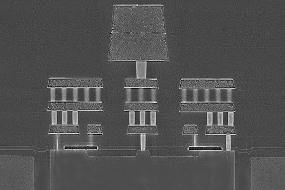
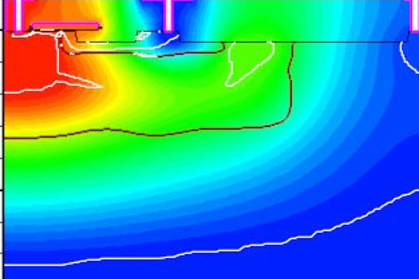
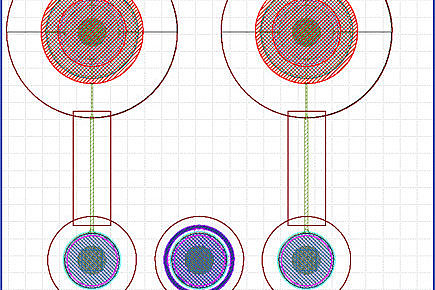
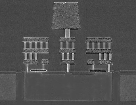
Galvanic isolation solutions
Our galvanic isolation process technology enables the fabrication of robust and reliable HV signal isolation solutions and achieves best-in-class isolation performance.
Key features of our galvanic isolation process solutions are:
- Barrier laid out for working voltages up to 1700 V
- Designed for operating temperatures of up to 175 °C
- Supports both capacitive and inductive coupler implementations
- Evaluation test structures available
- Best-in-class PDK support for all major EDA vendors


Related Resources
Contact

Tilman Metzger
Technical Marketing Manager
High Voltage
For more information, please contact us: