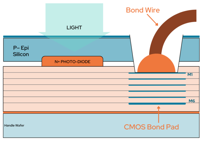
X-FAB Silicon Foundries SE, the leading analog/mixed-signal and specialty foundry, has just announced a major addition to its optical sensor offering. Aimed at use in next generation image sensor fabrication, the company is now able to provide a back-side illumination (BSI) capability in relation to its popular XS018 180nm CMOS semiconductor process.
Through BSI, imaging devices’ performance characteristics can be significantly enhanced. It means that the back-end process metal layers do not block the incident light from reaching the pixels, increasing fill factors by up to 100%. This is highly beneficial in situations of low-level illumination – as higher pixel light sensitivity can be achieved. BSI also offers the added advantage of significantly reducing the crosstalk between neighboring pixels, due to shorter light paths, leading to better image quality. Though small-pixel BSI solutions for 300mm wafers with high-volume consumer usage are commonplace, there are very few options available for image sensors with stitched large-pixel arrangements for 200mm wafers, especially when additional customizations are required. The new X-FAB BSI capability brings new possibilities, allowing customers with even the most demanding application expectations to be served - such as those involved in X-Ray diagnostic equipment, industrial automation systems, astronomical research, robotic navigation, vehicle front cameras, etc.
Leveraging the XS018 platform, which offers high readout speeds and exhibits low dark currents, image sensors with multiple epi options will be produced. An ARC layer can be added and then tuned in accordance with particular customer requirements. The accompanying X-FAB support package covers a full workflow from initial design through to the shipment of engineering samples, with a comprehensive PDK included.
“BSI technology has become increasingly prevalent in modern imaging devices, thanks to its ability to boost image quality by placing light-sensitive elements closer to the light source and avoiding unwanted circuitry obstructions. This is proving very useful in environments where light is limited,” states Heming Wei, Technical Marketing Manager for Optical Sensors at X-FAB. “Though much of this uptake has been within the consumer electronics sector, there are now numerous opportunities emerging in the industrial, automotive and medical markets. Via access to X-FAB’s BSI foundry solution, it will now be possible for these to be properly attended to, with a compelling offering being provided that brings together heightened sensitivity, enlarged image sensor dimensions and bigger pixel capacities too.”
- END -
Acronyms
ARC - Anti-Reflective Coating
BSI - Back-Side Illumination
CMOS - Complementary Metal Oxide Semiconductor
PDK - Process Design Kit
About X-FAB
X-FAB is the leading analog/mixed-signal and MEMS foundry group manufacturing silicon wafers for automotive, industrial, consumer, medical and other applications. Its customers worldwide benefit from the highest quality standards, manufacturing excellence and innovative solutions by using X-FAB’s modular CMOS and SOI processes in geometries ranging from 1.0 µm to 110 nm, and its special silicon carbide and MEMS long-lifetime processes. X-FAB’s analog-digital integrated circuits (mixed-signal ICs), sensors and micro-electro-mechanical systems (MEMS) are manufactured at six production facilities in Germany, France, Malaysia, and the U.S. X-FAB employs more than 4,200 people worldwide.
X-FAB Press Contact
Anja Noack
MarCom Manager
X-FAB Silicon Foundries
+49-361-427-6162
anja.noack@xfab.com

