Sensors
The real world is analog, but the world we live in is becoming more and more digitized. That is why sensors are getting increasingly important and essential to connect the analog world with the digital world.
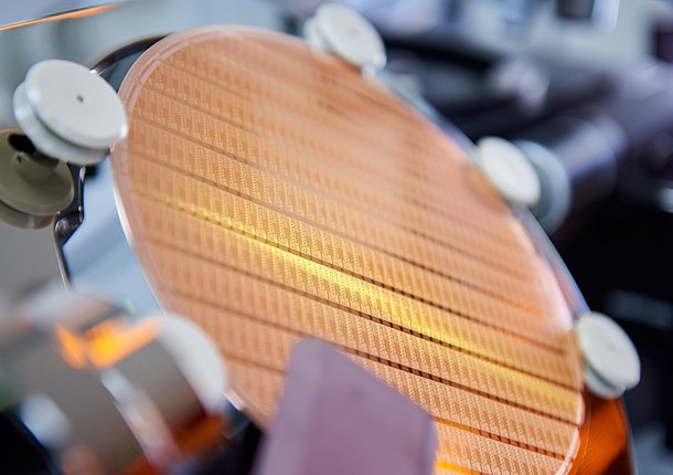
At X-FAB, we provide a comprehensive range of sensors measuring light, pressure, temperature and others. Our sensor wafer production is based on high-volume technologies and fulfills automotive standards. Our best-in-class ultralow-noise CMOS technologies – XH035 and XH018 – are recognized and adopted by tier-one semiconductor vendors for sensor interfaces.
Our sensors and sensor interfaces can be highly integrated, combining analog precision, low noise, an extensive range of photodiodes, (micro electronic mechanical systems) MEMS elements and 3D integration. Our MEMS processes, include various non-CMOS compatible processes such as noble metals and/or the creation of moving MEMS sensors through selective removal of silicon or the addition of other structural layers.
Apart from the wide variety of technical features and integration possibilities, we support our sensor technologies for the long term which perfectly suits the automotive, medical and industrial markets.
50% of all cars with a tire pressure monitoring system (TPMS) have MEMS pressure sensors made by X-FAB
Applications

Ambient light sensors
Like the human eye, ambient light sensors detect the brightness of the environment. They are used in all mobile phones to control the display brightness.
In addition to integrated photodiodes with high sensitivity in the spectral range of the human eye, we offer leading low-noise transistors for amplification as well as trimming devices to adjust important parameters.
Air intake gas sensors
The great advantage of using gas sensors, for instance to control the air intake in vehicles, is that it is very selective and able to measure toxic gases that the human nose cannot detect. The air intake gas sensors detect levels of CO and NOx in traffic and provide data for automatic HVAC air intake control. If the outside air quality is below acceptable levels, the cabin ventilation system automatically turns off the intake of outside air and switches the internal circulation ventilation system on.

Contactless thermometer
Our medical-grade thermopile MEMS processes are used in handheld consumer goods to measure at a safe distance whether people have elevated temperature. This is a safe and efficient way to determine whether individuals show symptoms of COVID-19.

Manifold absolute pressure sensor
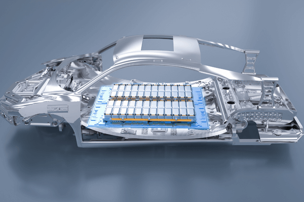
Manifold absolute pressure (MAP) sensors are used in the electronic control systems of fuel-injected internal combustion engines. The MAP MEMS sensor provides instantaneous manifold pressure information to the engine’s electronic control unit, which is used to calculate the air density and determine the engine’s air mass flow rate. This in turn determines the required fuel metering and influences the advance or retard of ignition timing, thus ensuring optimum combustion and contributing to a more sustainable world.
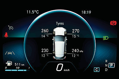
Smart TPMS MEMS sensors
The new generation of tire pressure monitoring systems (TPMS) in cars includes two MEMS sensors: a pressure sensor and an inertial sensor. The great advantage of this is that it ensures a longer lifetime of the system itself and provides additional information beyond conventional tire pressure measurements. This increases safety and optimizes fuel economy, longer tire life expectancy and greater comfort.
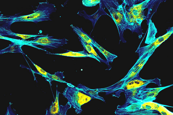
Fluorescence lifetime imaging
Lab-on-a-chip technologies enables a fast and smart solution on the point-of-care. One important method within this bio-medical application is time-resolved fluorescence or lifetime imaging micorscopy. It needs the observation of signal decays which could be very short. The low timing jitters of our SPAD (Single Photon Avalanche Diodes) allows the detection of these short time light pulses.
Optocoupler
An optocoupler allows the transfer of electrical signals between two isolated circuits by light. They are commonly used in electrical cars to control high-voltage batterie power. Typical optocoupler consist by a light source (LED or laser diode) and an optical receiver (photodiode). A special requirement is an electric shielding in the light path. With our large portfolio of photodiodes we can support different kinds of optocoupler.

Position sensor
Position sensors are used to detect the distance (linear encoder) or angle of a rotary part (rotary encoder). They are widely used in automotive and industrial applications. We provide a wide range of sensors for this application and support the often-unique layout requirements of such sensors or sensor arrays.
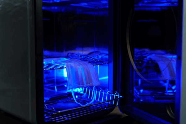
UV sensing
UV-sensors are used in health and industrial applications to control the UV exposure. UV purification has become more important in recent years. Our sensors allow a well control of the used UV dose. UV-sensors as part of mobile phones or wearables allow the measurement of the personal UV exposure to avoid sunburn or skin diseases like cancer. We are offering reliable photodetector for UV A, B and C with best sensitivity (>50 % quantum efficiency for UV-A, 40 % for UV-B and 35% for UV-C).

X-ray
X-ray sensors need large pixels. In contrast to the small pixels used in consumer products such as mobile phones and digital cameras, larger pixels have specific challenges regarding charge collection. Speed issues and image lag being more likely for large pixel. Our reference designs help you meet these challenges.
More than 20% of mobile phones manufactured worldwide feature an ambient light sensor made by X-FAB.
Solutions
- APD/SPAD
Our avalanche photodiodes (APDs) and single-photon avalanche diodes (SPADs) can be used in consumer, automotive and medical applications. APDs and SPADs are part of our highly modular, automotive qualified process XH018 and completely integrated in the design kit.
We offer primitive devices for our APD in linear mode which are scalable from 30 µm to 200 µm, and for our SPAD in Geiger mode with sizes from 10 µm to 30 µm. Models for optical and electrical simulation, along with a specific application note, help to easily integrate these devices into your IC.
Our SPADs feature a high photon detection probability over a wide wavelength range and an excellent low dark count rate. A short dead time lower than 3 ns results in a high bandwidth.

Webinar on APD/SPAD Webinar on APD/SPAD 
Layout of an X-FAB APD 
X-FAB's SPAD evaluation chip with quenching circuit - Gas & flow sensors
Our gas and flow sensors are based on our well-established noble-metal processes, especially the platinum metallization process. The advantage of using MEMS processes for these types of sensors is that the resulting sensors are very small, while still offering the performance of currently available medical or industrial sensors. This enables a wide range of applications that cannot be addressed so far using conventional gas or flow sensors. Together with backside etching (dry or wet), the platinum metallization process allows the technologies required to manufacture our MEMS gas and flow sensors. The operating principle relies on a heated platinum structure, whose reaction with the environment results in an electrical signal that can be used for direct or indirect flow or gas sensing.

- Image sensors
Unlike the small-sized four-transistor pixels used in consumer products such as mobile phones and digital cameras, our XS018 technology is the first to support the large high-speed pixels required for medical and scientific applications such as computer tomography and X-ray scanners for 3D images.
The XS018 process supports pixel sizes up to 200 µm x 200 µm with high-speed reading capability. XS018 has a 3.3 V core that results in a very low mask count, reducing costs when 1.8 V devices are not necessary. Optionally, it can be extended for higher integration by using a 1.8 V module.
Our four-transistor pixel cells with pinned photodiodes offer low dark current and low noise. The pinned photodiode available with four different pinning voltages and a 3.3 V n-channel MOS transistor with five different options for low-threshold voltages can be used as source follower, reset device or row select device in the pixel, making it easier for designers to find the right device for their applications. If your design doesn’t fit the maximum reticle size, our stitching capabilities for large dies could help you.

Circuit of transistor pixel cell 
Cross section of a transistor pixel cell - Inertial sensors
Our inertial sensor offering covers both accelerometers and gyroscopes in the X,Y and Z axes. All of them satisfy automotive quality standards, ensuring that our customers are supplied with well-functioning devices that meet their requirements.
The sensing is enabled through the movement or bending of robust single-crystalline silicon structures in the X, Y and Z planes, suspended within in a sealed cavity. The silicon sensing features are formed using a dry etching process, while low stiction of moving parts is achieved through a well-controlled and engineered release process. Furthermore, our trench-filled isolation technology provides low parasitic capacitance. We achieve hermetically sealed devices with well-established wafer-level packaging processes, allowing customers to select a range of cavity pressures. Depending on the accuracy and sensitivity required, inertial sensors can be based on either SOI or bulk silicon technology.


X-FAB’s has its own open platform technology XMB10 for inertial MEMS sensors. It is our main inertial sensor technology and best suited for 1 to 3-Axis Inertial Sensor applications, enabling acceleration sensors and gyroscopes. Other, more exotic applications which require movable structures can also be manufactured using the XMB10 process technology. This was showcased during various design competitions Fore more information on the features, applications and design and simulation support available for the XMB10 watch the recorded webinar session from EUROPRACTICE:
- Photodiodes
Our characterized photodiodes are integrated in modular process platforms and can be combined with dozens of other technology modules using high-running reliable processes with internal second source. The photodiodes span the entire wavelength spectrum optimized for UV, visible and near-infrared light. Our latest generation offers the industry’s highest UV-responsivity for integrated photodiodes. The quantum efficiency for visible light is higher than 90%.
They are part of our process design kits and can be implemented as sensor elements like any other electrical device. Our models enable the simulation of electrical and optical parameters. Specific application notes as well as our unique support in photodiode matching, will help you to optimize your optical sensor design.
Integrated photodiodes are available in our 180 nm technologies XS018, XH018 and our 350 nm technology XO035. Special support for optical sensors, like optical window etching and antireflective coating, is also available in several other processes.
Layout of X-FAB Photodiode evaluation chip - Pressure sensors
We have been manufacturing MEMS pressure sensors for over 25 years, which reflects our mature offering and expertise in this field. Our pressure sensor technology includes relative and absolute pressure sensors using a wide range of processes, enabling us to provide a complete range of pressure sensors for any automotive, industrial and medical applications.
Our sensing elements are based on piezo sensitive implants and wet or dry backside etching to free up the actual membrane structures. To accommodate different pressure ranges and sensitivities, we offer membranes made out of bulk, EPI or SOI silicon wafers. Our processes provide pressure sensors for all kinds of media including corrosive and high temperature environments required for some automotive applications. This is to ensure compliance with the latest and strictest environmental legislation requirements.


- Temperature sensors
Our infrared sensors are based on the thermopile principle. Depending on the customer design, these can be single- or multiple-pixel thermopiles. The advantage of our temperature sensors is that they can provide medical-grade and contactless measurements, which is especially important in the current COVID-19 era. The wafer process to manufacture these thermopiles requires a well-controlled wet etching process to ensure that the appropriate sensitivities and functionality can be achieved. X-FAB offers both discrete and integrated solutions based on the XH035 CMOS technology. Despite increasing the complexity of the overall technology, the integrated solution provides great advantages as the device size can be significantly reduced.

Our Commitment
Quick time to market through modularity: Our sensor technologies can be easily designed using the module or process blocks available.
Excellent support and expertise in the sensor world: Our staff and company structure ensure that our customers are successful in the competitive and innovative semi-conductor industry.
Reliability: Our sensor wafer production is based on high-volume technologies and automotive standards.

Long-term partners: We provide long-term support for our sensor technologies perfectly suitable for the automotive, medical and industrial markets.

We are convinced that the economy of the future will be sensor-based. As a specialist foundry, we are well placed to provide the sensor technologies required to enable this exciting future.
Stijn Sampermans, Product Marketing Manager, BU MEMS

Related Resources
Contact

Heming Wei
Technical Marketing Manager
Sensors
For more information, please contact us: