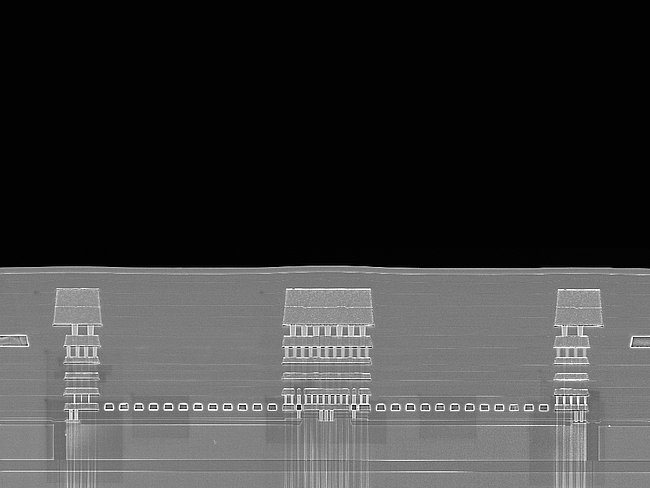
X-FAB Silicon Foundries SE, the leading analog/mixed-signal and specialty foundry, today announced the availability of second generation XT018 superjunction high-voltage (HV) primitive devices. Covering a voltage range from 45 V to 375 V, these devices are targeted at applications such as medical ultrasound transmitter/receiver ICs and AC line powered IoT sensors.
The new complementary NMOS/PMOS devices are based on the company’s XT018 advanced 180 nm BCD-on-SOI platform with deep trench isolation (DTI). Fully qualified for an extended temperature range of -40˚C to +175˚C, they can be incorporated into automotive AEC-Q100 Grade 0 products. They deliver industry-leading on-resistance (R(ds)on) figures, while still providing robust safe-operating areas for R(ds)on, Idsat and Vt. The complete voltage range up to 375 V is covered via use of a single process module.
BCD-on-SOI technologies are attractive to designers due to the superior attributes they have when compared to bulk BCD technologies. Key benefits of this approach include effectively latch-up free circuits, enhanced EMC performance and simplified handling of below ground transients. BCD-on-SOI allows significant die size area reductions, resulting in cost advantages over bulk BCD.
For the first time, customers are now able to design highly integrated ICs which can be directly powered from 230 V AC mains. This opens up an alternative power option to the increasing number of IoT edge nodes now starting to be deployed – allowing the power budget constraints of battery use to be avoided. Combined with the qualified XT018 eFlash, smart IoT device implementations are also possible.
Medical ultrasound transmitter/receiver ICs require well-matched HV NMOS and PMOS devices in terms of their R(ds)on and Idsat. In response to this, X-FAB has also released a new low R(ds)on PMOS module. This module comes with new PMOS primitive devices capable of supporting operating voltages up to 235 V. These HV PMOS primitive devices feature a 40% reduction in R(ds)on compared to regular 2nd generation superjunction PMOS devices.
As Joerg Doblaski, X-FAB’s CTO states: “The qualification of our leading 180 nm BCD-on-SOI technology platform up to 400 V is a big step for X-FAB and our customers. With the flexibility to freely float low and high-voltage primitive devices, our customers will be empowered to design a wide variety of new innovative products.”
###
About X-FAB
X-FAB is the leading analog/mixed-signal and MEMS foundry group manufacturing silicon wafers for automotive, industrial, consumer, medical and other applications. Its customers worldwide benefit from the highest quality standards, manufacturing excellence and innovative solutions by using X-FAB’s modular CMOS and SOI processes in geometries ranging from 1.0 µm to 130 nm, and its special silicon carbide and MEMS long-lifetime processes. X-FAB’s analog-digital integrated circuits (mixed-signal ICs), sensors and micro-electro-mechanical systems (MEMS) are manufactured at six production facilities in Germany, France, Malaysia and the U.S. X-FAB employs about 4,000 people worldwide.
X-FAB Press Contact
Thomas Hartung
VP Sales & Corporate Marketing
X-FAB Silicon Foundries
+49-361-427-6160
thomas.hartung@xfab.com
Acronyms
BCD Bipolar CMOS DMOS
DTI Deep Trench Isolation
EMC Electro Magnetic Compatibility
HV High-voltage
IC Integrated Circuit
Idsat Saturated drive current
NMOS Negative channel Metal-Oxide Semiconductor
PMOS Positive channel Metal-Oxide Semiconductor
R(ds)on Drain-source on resistance
SOI Silicon-on-Insulator
Vt Threshold voltage

