X-FAB Silicon Foundries, the specialty foundry for analog/mixed-signal and optoelectronic solutions, has made augmentations that extend the scope of its XS018 180 nm sensor process.
As a result, the company is now able to offer a photodiode-specific process core module. Whereas previously the XS018 process had been mainly focused on the fabrication of multi-pixel CMOS image sensors, this new module is dedicated to photodiode fabrication.
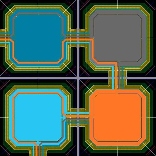
Through this module, X-FAB is now in a position to offer customers six different photodiode options. These cover wavelengths from ultra-violet (UV) right through to near-infra-red (NIR). The diverse operational parameters of the photodiodes in this family means that they can be aligned with various customer application requirements. X-FAB will be hosting a free webinar that gives details of the augmented XS018 process on Thursday, April 15th, 2021. There will be two sessions, one for Asian and European audiences, and another for attendees from the Americas. For more details and to register, click here.
The new X-FAB photodiodes are capable of delivering best-in-class UV sensitivity, attaining 40% quantum efficiency (QE) in the UVA band, 50-60% QE in the UVB band and over 60% QE in the UVC band. In relation to NIR, significant performance improvements have also been witnessed. At 850 nm the photodiodes have 17% greater QE than legacy devices based on the original XH018 process, and at 905 nm there is a 5% QE increase witnessed. With a QE of approximately 90%, the human eye response option is highly suited to ambient light sensing applications.
A unique feature means that photodiode responsivity can be stipulated, via specifying the size of the metal aperture. The output current of the photodiode is thereby scalable between full current and no current – in order that any differences caused by filtering can be compensated for. This in turn simplifies the accompanying amplification circuitry for photodiode arrays. Other enhancements include a 10% increase in the fill factor compared to devices based on the earlier XH018 generation. Through this, devices can be created that will respond to lower light levels, or the size of the die can be reduced in order to save space.
“Through ongoing investment, X-FAB has built up strong optoelectronic credentials. Among the proof points of this is the fact that over 20% of mobile phone handsets manufactured worldwide feature an ambient light sensor that was produced by us,” states Luigi Di Capua, VP of Product Marketing at X-FAB. “Thanks to the advances we have announced in relation to our photodiode offering, we will now be better positioned to address client demands for proximity sensing, spectral analysis and optical distance/triangulation measurement solutions.”
The six photodiodes are available as of now, through the “my X-FAB” customer portal. To learn more, please contact X-FAB sales, and they will provide you with further information.
###
About X-FAB
X-FAB is the leading analog/mixed-signal and MEMS foundry group manufacturing silicon wafers for automotive, industrial, consumer, medical and other applications. Its customers worldwide benefit from the highest quality standards, manufacturing excellence and innovative solutions by using X-FAB’s modular CMOS and SOI processes in geometries ranging from 1.0 µm to 130 nm, and its special silicon carbide and MEMS long-lifetime processes. X-FAB’s analog-digital integrated circuits (mixed-signal ICs), sensors and micro-electro-mechanical systems (MEMS) are manufactured at six production facilities in Germany, France, Malaysia and the U.S. X-FAB employs about 3,800 people worldwide. www.xfab.com.
X-FAB Press Contact
Thomas Hartung
VP Sales & Corporate Marketing
X-FAB Silicon Foundries
+49-361-427-6160
thomas.hartung@xfab.com
Acronyms
NIR Near Infra-Red
QE Quantum Efficiency
UV Ultra-Violet